Your photos show fabrication performance similar to the PCBWay order I placed back in January. The off-center drill hits certainly aren't bad enough to cause problems with manual assembly, and they probably conform to customary industry tolerances as well as the supplier's stated tolerance, but I can imagine being taken aside by a manufacturing engineer who wants to know if I expect the hole placement to improve with the next batch.. . . registration is good (still not perfect) . . .
The silkscreen looks ratty. Technical people tend to not care about this as long as it's legible and the edge irregularities don't lop over where they shouldn't be. Less enlightened souls (e.g., purchasing, sales, project management) often judge the "quality" of a board primarily on the silkscreen.
(I think your first photo shows a via too close to the edge of a copper fill. I'd expect the DRC in your layout software to squawk that, before the board goes to fab.)
Dale
I often place electrically unconnected pads on both top and bottom around unplated holes - often for holes used to mount the board itself, or where the hole receives a switch, connector, etc.If there is a pad drawn on both sides of the board for a heat sink, it should be there and through hole plated. . . .
Dale
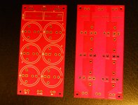
Latest PCB
Here is the latest pcb I had made, no traces at all, just copper pours. My capacitor bank, with 2 oz copper.
MI
Here is the latest pcb I had made, no traces at all, just copper pours. My capacitor bank, with 2 oz copper.
MI
Attachments
Last edited:
And if the instructions contradict OR DUPLICATE something else in the drawing package - i.e., there wasn't any reasonable "room for interpretation" before adding the instructions - errors will almost certainly occur sooner or later.If there's room for interpretation, instructions clarify things.
If your instructions resulted in errors, the instructions weren't clear. . . .
I have heard several manufacturers complain of "language barrier" problems when dealing with offshore suppliers of many types. I have never had a problem with misinterpretation of the short, very specific, to-the-point statements in drawing notes.
In the world of circuit board fabrication, Gerber files are the de facto arbiter of communication between designer and fabricator, to the extent that they can be. I always do at least a cursory, layer-by-layer as well as overlaid layers, review of Gerbers before ordering boards. I think once I actually found a drafting error I made in the original layout program. A few times I found errors in computer file administration - Gerbers from a prior revision, or Gerbers generated from working files rather than final files, got into the project directories. But there's enough anecdotal evidence about layout programs which DO NOT generate Gerbers correctly to make me paranoid about inaccurate Gerber files. (I seem to recall a squawk in KiCAD's bug tracking system about an error in generating Gerber files, but I can't find it right now.)
But Gerber files don't contain ALL the information about fabricating a board. That's why we need Excelon drill files. Having separate drill files for plated and unplated holes is one solution to the problem of differentiating the two types. It's clumsy, but if the fabricator prefers that method, then send him separate files! And if he hasn't settled on that method for dealing with the hole types, then don't confuse the guy by sending two files!
Dale, silkscreen is good, just looks "bad" under magnificaction. (Can't show more)
The via on the copper pour is not an issue.
The via on the copper pour is not an issue.
And if the instructions contradict OR DUPLICATE something else in the drawing package - i.e., there wasn't any reasonable "room for interpretation" before adding the instructions - errors will almost certainly occur sooner or later.
Well, this goes by:
. . . . Also, be aware that its almost expected you include a "README.TXT" or "INSTRUCTIONS.TXT" file, where you clearly spell out anything that could be questionable . . . .
In many cases, this file is REQUIRED - and not just for "questionable" information. I have attached a template for this file, based on an actual README.TXT file I recently submitted with a PWB order.
Dale
I often place electrically unconnected pads on both top and bottom around unplated holes - often for holes used to mount the board itself, or where the hole receives a switch, connector, etc.
Dale
This would require special instruction, but the common sense thing would be to not worry about it. Who cares if your screw holes are through plated or not. If this is a concern, then PCBWay isn't a good choice for you to have boards done.
Their product is good for a quick prototype or a quick and dirty DIY project, but not something you want to sit and admire all day. The silk is rough and the HASL is too thick for that.
I don't usually bother even adding a pad around the screw holes on mine. A screw will chew through 1oz copper if tightened and make a mess of it anyway. If HASL is selected for a surface finish, the pad will be blobbed with uneven solder and the board won't sit on the standoffs properly either. The epoxy of the FR4 is a superior surface for a fastener to contact. It isn't as easily damaged.
I care about unplated screw/mounting-holes as force might/will damage the plating. 🙂 (In case I need contact from the board to case) For good forced contact, I stitch the restring with vias and apply solder paste pattern to it, so the screw will finally wedge the solder.
If you care about unplanarity, go for ENIG.
If you care about unplanarity, go for ENIG.
As I said, if this sort of thing is a concern for you, then this likely isn't the right board house for you. They don't do boards meant to admire all day. They cater to prototypers and DIY enthusiasts. They don't cater to people who worry about how pretty the screw hole looks.
Putting a flat washer under the screw is a much simpler solution. Epoxy FRP is very resilient. Thin copper is not.
Putting a flat washer under the screw is a much simpler solution. Epoxy FRP is very resilient. Thin copper is not.
I agree. That's why I'm not that concerned about whether or not my screw holes are through plate. It doesn't really effect the sound.
Same here. Most of mine are potted in epoxy and used in automotive applications. Once it's assembled and put into service it will never be seen again. If there's a problem it goes in the garbage. Impossible to troubleshoot and repair.
Inner layers are 1oz copper!
Well here is another positive thing for pcbway. Their inner layers on 4 layer boards are 1 oz copper!
I spotted this in their fab specifications a few days ago and had them confirm. Seeed Studio, where I was having boards made previously, only uses 1/2 oz copper on the inner layers. 1/2 oz has forced me to nearly double the size of internal traces to compensate.
Here is what pcbway just emailed for their 4 layer detail for a 1.6mm board:
PCB DESCRIPTION:4 LAYER PCB 1.6 MM 1oz
Copper 1 35um (0.035MM)
Dielectric 1-2 0.175 mm (e.g. 1x Prepreg 7628 AT05 47% Resin)
Copper 2 35 um
Dielectric 2-3 1.2 mm (6x 7628M 43% Resin)
Copper 3 35 um
Dielectric 3-4 0.175 mm (e.g. 1x Prepreg 7628 AT05 47% Resin)
Copper 4 35 um
35uM = 1oz copper. By comparison here is Seeed's specification page
Fusion PCB Specification ? Feedback & Ideas for seeed
Scroll down to "Inner Layer Copper Thickness" and they list 0.017uM (0.5oz) for layers 2 and 3.
I can shrink some of my inner traces on the 4 layer board back to regular widths. 🙂
watch for price increases after the review!
Here is another experience I just had with pcbway.
I sent a new version of a 4 layer board in. The original price the system came up with was $119, $94 for 5 boards and the $25 DHL shipping. Then it goes into the "can't pay, board under reivew" phase. An hour later I check and find the price is now $26 higher, $145! I find a "?" icon by the price, which comes up with a "special technology" charge. What??
Then I find an email from customer service saying "your file contained two boards, so we have added the panelization fee".
Ummm... no. I then submitted the same Gerber files to Seeed Studio, where it was correctly identified as a single board. I went ahead and had Seeed process the board this time.
I replied to the customer service email about the problem. They said that they (re)checked the file and sure enough, one board, and they were not sure why their checker made the mistake.
Worse still, I've come to realize the same thing probably happened the other time I submitted this 4 layer board to them and I paid it without realizing. After the review I remember thinking the price seemed to be more than I remembered. But the increase was around $25, and shipping was around $25, so I assumed that original quote must have been without shipping and just paid it without checking. The only inidication the price had gone up after the review was the price number changed color to red and the small "?" icon showed up next to it.
Argh. At this point I'm unfortunately spooked about this outfit. I'll probably be sending future orders back to Seeed Studio.
Last edited:
agdr--- pcbway did a 4 layer board for me and I didn't have a problem. But in the past whene there was a problem with either the workmanship or layout, I found the language barrier unbearable. They are cheap, when you can use them. If you are interested though, the main contact I had at PCB way (who called himself "lambo") left and started his own PC board company a few years ago, and he's done some good work for me at prices competitive with PCB way. Don't know if he has a web site set up yet, so if you're interested send me a private msg, and I'll send you his email. I can vouch for the work, and though there is still a little language barrier, at least he does address concerns, and wants your business.
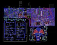
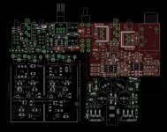
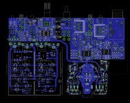
Would you mind to post your layout?
Sure thing. Below is the whole layout in the first image, then the 4 separated layers. It is this project:
http://www.diyaudio.com/forums/head...avguy-o2-headphone-amp-vs-original-thd-n.html
I have a theory that pcbway's scanning software "saw" that dashed line on the silk-screen half way up the board in the middle and decided it was a score/cut mark for two panels. The line is actually there because another board can bolt on top of this board in place of the batteries. The dashed line is just the extent of the add-on board.
Attachments

Last edited:
agdr--- pcbway did a 4 layer board for me and I didn't have a problem. But in the past whene there was a problem with either the workmanship or layout, I found the language barrier unbearable. They are cheap, when you can use them. If you are interested though, the main contact I had at PCB way (who called himself "lambo") left and started his own PC board company a few years ago, and he's done some good work for me at prices competitive with PCB way. Don't know if he has a web site set up yet, so if you're interested send me a private msg, and I'll send you his email. I can vouch for the work, and though there is still a little language barrier, at least he does address concerns, and wants your business.
Interesting! I'll send a PM. 🙂
To pcbway's credit they did email me right back last night, admitted the mistake, and were willing to work with me on submitting it again. But... in my view why go through all that when I don't have to. Coupled with the previous problem posted above of the pad on a heatsink missing on a 2 layer project - their error - which I also didn't have happen when that board was fabbed at Seeed. These folks have potential though. I'll probably try them again in a year.
Would guess your Gerbers aren't 100% correct. Even if you're done with pcb way, I'm interested in this problem and would like check your dataset, if you like.
- Status
- Not open for further replies.
- Home
- Design & Build
- Parts
- PCBway Ordering Experiences