10 boards are LESS than 5 sometimes!
Here is another related pcbway ordering surprise. I quoted 5 pieces today of a 80 x 120mm board, 4 layer 1.6mm HASL, and it came up $118 for the boards and $25 for DHL. Then I tried the same for 10 boards and it came up $101 for the boards and the same $25 for DHL - $17 less for 5 additional boards!
Then I tried quoting a shrink from 120mm to 100mm (80 x 100mm, 1.6mm, HASL) and WOW! The price for either 5 or 10 boards dropped all the way down to $49.
So it is definitely worth spending some time trying different things with their quoter.
Last edited:
i ordered 10 of 100x100mm, 2layer, standard $13 deal, even sent hkpost, as i was in no rush. received 11 in about a month, all with gold plating, good quality. now reworking more designs to fit 100x100
Gold plating? You ended up with an ENIG finish?
yes i received immersion or electrolysis nickel/gold as one of their plating options.
I guess if they have orders in for some enig pcbs, then they just lump everything together on the production panel, assuming the customer is fine with the plating option upgrade. In my case, it was acceptable to me, they even gave me 11 of them.
If you go over 100mm on any dimension the price goes up, quiet a bit as you will notice, so try your best to keep your pcbs at or under 100x100mm is the answer for the great deal.
Last edited:
Is there actually a "snail mail" option? DHL Express charges a lot of extra fees when shipping to Germany. (And they do (proven) wrong bills to rise their margin)
I used the HK post option, it worked out fine, takes a while but saves a few $ if you are in no rush.
they forward the order to someone in HK first, then that person posts them to the customers. Took about a month.
they forward the order to someone in HK first, then that person posts them to the customers. Took about a month.
yes i received immersion or electrolysis nickel/gold as one of their plating options.
I guess if they have orders in for some enig pcbs, then they just lump everything together on the production panel, assuming the customer is fine with the plating option upgrade. In my case, it was acceptable to me, they even gave me 11 of them.
If you go over 100mm on any dimension the price goes up, quiet a bit as you will notice, so try your best to keep your pcbs at or under 100x100mm is the answer for the great deal.
Sorry, I meant to ask did you specifically request ENIG finish or did you ask for normal HASL and they changed to ENIG?
I ask because when I change to ENIG at the time of quoting, it's not $13 but $37 + shipping for a 100x100mm FR4 dual-layer board
i ordered the special $13 USD deal, which by default is HASL using lead/tin solder.
Tell me next time you order and spec a 2 layer ENIG pcb. I will submit my order at the same time, chances are I will get ENIG again even if I spec'd and paid for HASL🙂
Tell me next time you order and spec a 2 layer ENIG pcb. I will submit my order at the same time, chances are I will get ENIG again even if I spec'd and paid for HASL🙂
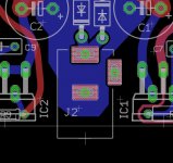
The board I sent is 4 layers and and is fairly large again, 120 x 130mm. Works just great. I've built it up and havent discovered any fabrication imperfections at all. No missing pads, no plating problems. This board has plated slots again for a power jack. Once again they came out just fine. I didn't send in any special manufacturing instructions for the slots either.
may I ask how the slots are defined in the gerbers? I need to do a board with PCBWAY that has slots so I'd like to know how to do that without "special instrunctions"
I believe the 10 for the same cost as 5 at pcbway only applies to boards less than 100x100mm.
I've had very good experiences with PCBWay. I've done a number of 2 layer boards and panellised boards (v scores need to be at least 70mm long). My latest board is 4 layer and is meant to be delivered this afternoon (I sent the order in last weekend). It is annoying that DHL charges about £11 to process £9 of VAT recovery for HMRC.
I've had very good experiences with PCBWay. I've done a number of 2 layer boards and panellised boards (v scores need to be at least 70mm long). My latest board is 4 layer and is meant to be delivered this afternoon (I sent the order in last weekend). It is annoying that DHL charges about £11 to process £9 of VAT recovery for HMRC.
How to make plated slots in Eagle
I actually haven't even had to look at the Gerbers, I did it all via Eagle. 🙂 The Eagle folks have warned me that the ability to process plated slots is very fab-specific. For instance last I looked at OSH Park's instructions they specifically state they don't do plated slots. But I've had boards with palted slots fabricated at both pcbway.com and seeedstudio.com (both China) now with no special instructions and the plated slots came out just fine.
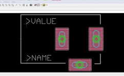
Here is how to do it in Eagle, in pictures (screen captures from Eagle). This may not help you much if you are doing slots by editing the Gerbers, but it may be useful to others out there using Eagle. The part here is the typical DC power jack (although this project uses it for AC), the switchcraft RAPC722X. The jack has 3 flat leads, one for +, one for -, and one for a switch contact. The rear flat lead is wider than the other two, hence one wider slot. Thanks, Switchcraft.
Photos and steps:
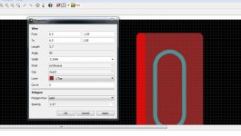
* The first two show the part on the layout, with the 3 slots. You are looking at quite a stack of stuff here on each slot. 🙂 There is a milled-out slot in the board (aqua), a rear foil polygon (blue, doesn't show), a top foil polygon directly on top of it (red), rear & front stop masks (the white hatching) and a pad. In the second image you can see one of the tricks: the hole in the pad has to be small enough to fit completely within the milled-out slot. The actual outer width of the pad donut isn't important, other than it should be (well) within the (red) top metal polygon but big enough to extend outside of the slot.
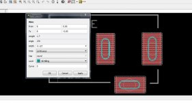
* The next image shows the part now in the package editor in Eagle. You bring this up by right clicking on the part in the layout and choosing "open package". Here I have the primary grid set at 0.1mm, with the alternate grid (hold down the ALT key) at 0.01mm. The grid lines that show up below then are 0.1mm. Again notice that rear slot has to be a bit wider than the rest.
* Next I've clicked on that milling layer oval and brought up the properties window. Here you can see the milling layer is on layer 46 in Eagle. The milled slots wind up in the .GML milling layer Gerber file, I believe. To make these slots I first drew two 0.127mm wide lines parallel to each other on layer 46. The minimum milling width at Seeed Studio and pcbway is 1mm, so that is the spacing I used between the lines, even though the jack datasheet called out for slightly thinner slots as I recall. Then with the arc tool I drew end caps bridging the two lines, also on layer 46 of course.
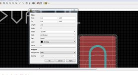
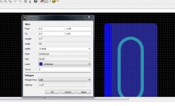
* Next up it is hard to see, but I've clicked on that white hatching at the top of the slot pad, which is the top stop mask layer (tstop), layer 29 in Eagle as that properties window show. I made the stop mask polygon extend 0.1mm past the top and bottom foil polygons, as can be read off the grid here. This tstop layer is sitting directly over the same thing for the rear of the board, the bstop layer on Eagle layer 30. I haven't shown that in any of the images here because it is an exact copy of this one. If I turned off this layer 29 in Eagle there it would be. 🙂
* Next I've turned off both of those stop layers, 29 & 30, and clicked on the top foil (red), Eagle layer 1, which from the bottom of the properties shows as a solid polygon. Once again directly under this one is the same exact thing on the bottom layer (blue, doesn't show because the top foil is covering it), Eagle layer 16, which is the next image. I turned off the top red layer so the bottom blue layer would show.
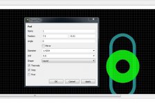
* Finally the pad. I've turned off both front and rear foil layers here. In this case the pad has a 0.6mm drill hole with a 1.42mm donut. The pad is required so there is something for the wiring to connect to on the part in the schematic.
And that is it! Works great. 😀 I've examined the interior plating inside the slot with a magnifying glass. Just perfect from either company (seeed or pcbway).
It did take me 3 tries on different projects (all use that same power jack) to optimize the slot width though, since the flat leads on the Switchcraft part also taper at the bottom, which allows the slot width to be even a bit less wide than it would seem. I started with the slot dimensions given in the jack datasheet and found the part was still able to wiggle a tiny bit back and forth in the slots. On the second try I shortened the width of the ends of all 3 slots by 0.5mm. Helped quite a bit when the second fab run came back! On the third try I shortened them another 0.5mm on each and and the result is just perfect. The part flat leads go in the slots with no scraping, yet the part doesn't allow much "wiggle" and stay oriented perfectly while soldering the leads.
may I ask how the slots are defined in the gerbers? I need to do a board with PCBWAY that has slots so I'd like to know how to do that without "special instrunctions"
I actually haven't even had to look at the Gerbers, I did it all via Eagle. 🙂 The Eagle folks have warned me that the ability to process plated slots is very fab-specific. For instance last I looked at OSH Park's instructions they specifically state they don't do plated slots. But I've had boards with palted slots fabricated at both pcbway.com and seeedstudio.com (both China) now with no special instructions and the plated slots came out just fine.
Here is how to do it in Eagle, in pictures (screen captures from Eagle). This may not help you much if you are doing slots by editing the Gerbers, but it may be useful to others out there using Eagle. The part here is the typical DC power jack (although this project uses it for AC), the switchcraft RAPC722X. The jack has 3 flat leads, one for +, one for -, and one for a switch contact. The rear flat lead is wider than the other two, hence one wider slot. Thanks, Switchcraft.
Photos and steps:
* The first two show the part on the layout, with the 3 slots. You are looking at quite a stack of stuff here on each slot. 🙂 There is a milled-out slot in the board (aqua), a rear foil polygon (blue, doesn't show), a top foil polygon directly on top of it (red), rear & front stop masks (the white hatching) and a pad. In the second image you can see one of the tricks: the hole in the pad has to be small enough to fit completely within the milled-out slot. The actual outer width of the pad donut isn't important, other than it should be (well) within the (red) top metal polygon but big enough to extend outside of the slot.
* The next image shows the part now in the package editor in Eagle. You bring this up by right clicking on the part in the layout and choosing "open package". Here I have the primary grid set at 0.1mm, with the alternate grid (hold down the ALT key) at 0.01mm. The grid lines that show up below then are 0.1mm. Again notice that rear slot has to be a bit wider than the rest.
* Next I've clicked on that milling layer oval and brought up the properties window. Here you can see the milling layer is on layer 46 in Eagle. The milled slots wind up in the .GML milling layer Gerber file, I believe. To make these slots I first drew two 0.127mm wide lines parallel to each other on layer 46. The minimum milling width at Seeed Studio and pcbway is 1mm, so that is the spacing I used between the lines, even though the jack datasheet called out for slightly thinner slots as I recall. Then with the arc tool I drew end caps bridging the two lines, also on layer 46 of course.
* Next up it is hard to see, but I've clicked on that white hatching at the top of the slot pad, which is the top stop mask layer (tstop), layer 29 in Eagle as that properties window show. I made the stop mask polygon extend 0.1mm past the top and bottom foil polygons, as can be read off the grid here. This tstop layer is sitting directly over the same thing for the rear of the board, the bstop layer on Eagle layer 30. I haven't shown that in any of the images here because it is an exact copy of this one. If I turned off this layer 29 in Eagle there it would be. 🙂
* Next I've turned off both of those stop layers, 29 & 30, and clicked on the top foil (red), Eagle layer 1, which from the bottom of the properties shows as a solid polygon. Once again directly under this one is the same exact thing on the bottom layer (blue, doesn't show because the top foil is covering it), Eagle layer 16, which is the next image. I turned off the top red layer so the bottom blue layer would show.
* Finally the pad. I've turned off both front and rear foil layers here. In this case the pad has a 0.6mm drill hole with a 1.42mm donut. The pad is required so there is something for the wiring to connect to on the part in the schematic.
And that is it! Works great. 😀 I've examined the interior plating inside the slot with a magnifying glass. Just perfect from either company (seeed or pcbway).
It did take me 3 tries on different projects (all use that same power jack) to optimize the slot width though, since the flat leads on the Switchcraft part also taper at the bottom, which allows the slot width to be even a bit less wide than it would seem. I started with the slot dimensions given in the jack datasheet and found the part was still able to wiggle a tiny bit back and forth in the slots. On the second try I shortened the width of the ends of all 3 slots by 0.5mm. Helped quite a bit when the second fab run came back! On the third try I shortened them another 0.5mm on each and and the result is just perfect. The part flat leads go in the slots with no scraping, yet the part doesn't allow much "wiggle" and stay oriented perfectly while soldering the leads.
Attachments

Last edited:
wow adgr,
thanks for the detailed explanation. I will study this in depth. since I also use Eagle, that should help a lot!
thanks again
thanks for the detailed explanation. I will study this in depth. since I also use Eagle, that should help a lot!
thanks again
The gerber data must create pads/ovals/shapes/keepouts etc to accommodate a slotmay I ask how the slots are defined in the gerbers?
but any drilling/milling of a slot is defined in the cnc excellon drill or milling data.
Another thing to consider is if the slot is to be plated or not? That will control the process of when the slot is created.
Some ecad tools do not create cnc milling data (which is a separate cnc file) so to make or specify a slot you have to create a hole in the centroid of a slot. Then in the drill schedule notes you specific a unique hole so that you get a separate entry in the drill schedule where you define the slot width(which is the drill hit or tool diameter) and the slot length.
pcbway in their cheap process by default plates all the holes or slots as they do not do secondary drilling/milling (non plated through holes) after plating. They only mill for image removal from the production panel.
Last edited:
pcbway assembly services
I've noticed that pcbway has board assembly services listed too. I just had an opportunity to quote their assembly services due to an incredibly tiny chip I'm considering using in a project. I need to kick out several copies to put the boards in parallel. Seemed like something to quote since I could have the board fabricated and assembled all by the same outfit.
The board is a 25mm x 25mm 2 layer, 0402 parts with the exception of that chip and some through holes. The quote for 15 boards came back as:
* Board fab $15
* Parts cost $136. They have the option of sending them the parts or they supply the parts. I was surprised here since their number is the same or less than what I would pay for small quantities (qty 25 or 50) at Mouser. I was expecting to send them my parts, but now I might consider using theirs.
* Assembly $155. Playing around with the quoter the price was the same (within $2) for quantity 5 as for qty 20. I guess the one-time setting-up of the assembly machines is most of the cost.
* Shipping $25 DHL, same as it would be for just the bare boards
* Paypal fee $16
Pretty impressive! I'll probably hand assemble the first couple versions, tiny chip or not, just to make sure it works. But I'm going to seriously consider the machine assembly for the final version, given the reasonable cost.
Last edited:
Well this should be interesting. I've sent in another 2 boards to PCBway, and this will be the second time one of my boards its an oddball. Its to be used as a control panel, so I'm mainly interested in the black solder mask, the drill holes, and the silk screen. They did one of these before for me and it was "mostly" OK, excpet that they added their job ID number to the lower bottom of the silkscreen, which is less then desirable when you're making something intended to be fully visible. I've asked them not to do this in my instructions, but another wrinkle is that this board has a few rectangular cutouts, and also does have a bottom copper layer, done as a copper pour, mainly for use as extra shielding for another board that gets mounted below. I spelled out my instructions pretty plainly, but it will be a real test of the language barrier.
One disturbing thing is that today they sent me a "thank you" for my order, along with a compressed (RAR) file containing what they called a "manufacture file", asking me to check it. That file contains files with names like ts,tl,ko,drl,bs, and bo, aalong with an additional compressed TAR file, containing another hundred files, several with identical names, and then there are more compressed files within that one.
I found this a bit upsetting, and i don't want to have to be responsible for figuring out what all these files are or what software to use to examine them. Even if I did, it looks like days of work to figure it it. I basically responded saying I did not know what the files were and have no software to open them. If we can't get adequate English communication to clarify what I need, this may be case where I'll have to forgo the bargain basement prices of PCBWAY.
Stay tuned.
I'll bet these are Gerber files. Open with "Gerbv" or your favorite Gerber viewer. Or just drop it into a common text editor (e.g., "Notepad++") to verify that it IS a Gerber file. You may find some useful metadata masquerading as comments.. . . One disturbing thing is . . . a compressed (RAR) file containing what they called a "manufacture file", asking me to check it. That file contains files with names like ts,tl,ko,drl,bs, and bo, . . . .
"TS" sounds like "Top soldermask" (and "BS" is the bottom); "TL" may be "Top legend" (i.e., silkscreen); "BO" could be "Board outline", etc.
For reference, the first few lines of a Gerber file created under the current file definition standard looks like:
G04 #@! TF.FileFunction,Copper,L2,Bot,Signal*
%FSLAX46Y46*%
G04 Gerber Fmt 4.6, Leading zero omitted, Abs format (unit mm)*
G04 Created by KiCad (PCBNEW (2016-03-13 BZR 6620, Git 44fc6cb)-product) date 14/03/2016 15:38:58*
%MOMM*%
G01*
G04 APERTURE LIST*
%ADD10C,0.152400*% . . . .
%FSLAX46Y46*%
G04 Gerber Fmt 4.6, Leading zero omitted, Abs format (unit mm)*
G04 Created by KiCad (PCBNEW (2016-03-13 BZR 6620, Git 44fc6cb)-product) date 14/03/2016 15:38:58*
%MOMM*%
G01*
G04 APERTURE LIST*
%ADD10C,0.152400*% . . . .
I can't begin to guess at these.. . . . along with an additional compressed TAR file, containing another hundred files, several with identical names, and then there are more compressed files within that one. . . . .
Dale
I'll bet these are Gerber files. Open with "Gerbv" or your favorite Gerber viewer. Or just drop it into a common text editor (e.g., "Notepad++") to verify that it IS a Gerber file. You may find some useful metadata masquerading as comments.
"TS" sounds like "Top soldermask" (and "BS" is the bottom); "TL" may be "Top legend" (i.e., silkscreen); "BO" could be "Board outline", etc.
For reference, the first few lines of a Gerber file created under the current file definition standard looks like:
G04 #@! TF.FileFunction,Copper,L2,Bot,Signal*I can't begin to guess at these.
%FSLAX46Y46*%
G04 Gerber Fmt 4.6, Leading zero omitted, Abs format (unit mm)*
G04 Created by KiCad (PCBNEW (2016-03-13 BZR 6620, Git 44fc6cb)-product) date 14/03/2016 15:38:58*
%MOMM*%
G01*
G04 APERTURE LIST*
%ADD10C,0.152400*% . . . .
Dale
I appreciate that Dale. And I'm not being lazy, but I guess I'm looking at this with the bigger picture of communication in mind. I've supplied boards like this to other China based companies before, and yes there were questions. But the questions came as simple English questions, or occasionally a simple graphic (JPG, PNG, GIF, etc) with arrows and questions. Never before has someone replied with hundreds of files, compressed files within files compressed with different methods, and told me to please "check". And I certainly don't want to try to hand parse files like this.
In response to my explaining that I had no software to examine these file, I got a terse response: CAM350 / Genesis software can open it! Pls check it."
So at this point I responded a little more strongly: "I can not check these files. I don't have either of the programs you mentioned, and would not know how to use them anyway. I supplied my gerbers and written instructions, and can answer questions if anything is not clear. If there is a question, just send me a simple graphic file marked with your questions. If we can't communicate based on this, you'll have to refund my money."
I also requested a specific salesperson, Daphne, get involved, as her communication skills were much better. But I suspect this is a case where they will just refund my money along with a simple "thank you for using PCBWAY".
I don't know what to suggest. I agree that PCBWAY isn't communicating their request with enough detail to get a complete, meaningful, response from you.
Depending on how many PCBs people want and where you're located, I will now recommend Quick Circuits - they're a local UK company (about 1 mile from my front door) and I used them for Bruno's Preamp group buy (see my sig).
I really appreciate the quality of their work, it's very very good. They are also remarkably cheap for a small, independent outfit.
Assembly costs a bit more with a low volume due to the creation of a solder paste stencil, but if you just want bare PCBs, they're worth a call maybe. On a batch of 100x 150mm x 50mm PCBs, it came out at around USD 5 per board, and that's of course for a proper RoHS, ENIG dual layer...
English people, with English patience and politeness, ISO9001, RoHS, etc, all top notch.
In fact, during the group buy, I hadn't given them positional P+P data which they needed of course for their pick and place machine. I eventually managed to get one over to them, but as they wanted to finish the job, they went out and bought some specialised software which reverse-engineered the Gerber data to create the missing P+P data. There was of course a cost to that software, but they didn't charge me anything for it - just took it on as a future investment.


Quick Circuits | PCB Manufacture & Assembly
I really appreciate the quality of their work, it's very very good. They are also remarkably cheap for a small, independent outfit.
Assembly costs a bit more with a low volume due to the creation of a solder paste stencil, but if you just want bare PCBs, they're worth a call maybe. On a batch of 100x 150mm x 50mm PCBs, it came out at around USD 5 per board, and that's of course for a proper RoHS, ENIG dual layer...
English people, with English patience and politeness, ISO9001, RoHS, etc, all top notch.
In fact, during the group buy, I hadn't given them positional P+P data which they needed of course for their pick and place machine. I eventually managed to get one over to them, but as they wanted to finish the job, they went out and bought some specialised software which reverse-engineered the Gerber data to create the missing P+P data. There was of course a cost to that software, but they didn't charge me anything for it - just took it on as a future investment.
Quick Circuits | PCB Manufacture & Assembly
Last edited:
- Status
- Not open for further replies.
- Home
- Design & Build
- Parts
- PCBway Ordering Experiences