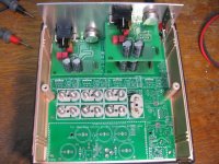
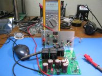
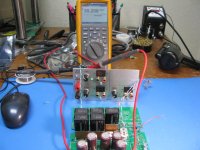
V1.0 boards back...
The boards for this project are back and... a few mechanical screw-ups so I'm not going to post the Gerbers quite yet. 🙂
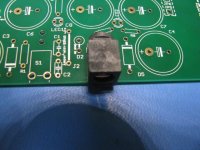
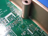
I missed a measurement on the Hammond 1598EBK mechanical diagram. The two side notches are not perfect half round 6.3mm radius, they are offset 2.87mm to form a notch. Easily taken care of in 30 seconds with a file on these boards, but still a screw-up.
A bigger hiccup is the ground screws on the bottom two Victor boards, and their washers, hitting the top of the power supply board. How did do that. 😡 I thought I had left 2mm between the two but apparently not. So hence the two filed-in notches on the front of the board in the photos below. I'll probably just mill out a section under the front of the Victor boards on the next board run to deal with it.
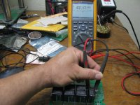
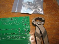
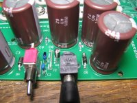
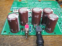
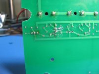
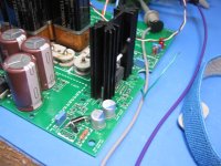
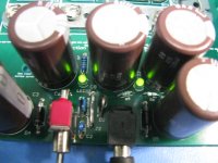
But at least it works electrically so far. The photos below show building up the end-mount battery snaps. After soldering each one in I used the nippers in the photo to cut off the excess. The primary cells shown stand nice and vertical. But some types of NiNH rechargeables have the negative snap sunk 0.5mm lower than the other. That's OK, the row "leans" a tiny amount in one direction and I've allowed for that.
The photos also show how to use the snaps as "shorting snaps" to short one or more of the battery positions This particular set is giving 67.17Vdc / 7 = 9.6Vdc each rather than 9.0Vdc.
The boards for this project are back and... a few mechanical screw-ups so I'm not going to post the Gerbers quite yet. 🙂
I missed a measurement on the Hammond 1598EBK mechanical diagram. The two side notches are not perfect half round 6.3mm radius, they are offset 2.87mm to form a notch. Easily taken care of in 30 seconds with a file on these boards, but still a screw-up.
A bigger hiccup is the ground screws on the bottom two Victor boards, and their washers, hitting the top of the power supply board. How did do that. 😡 I thought I had left 2mm between the two but apparently not. So hence the two filed-in notches on the front of the board in the photos below. I'll probably just mill out a section under the front of the Victor boards on the next board run to deal with it.
But at least it works electrically so far. The photos below show building up the end-mount battery snaps. After soldering each one in I used the nippers in the photo to cut off the excess. The primary cells shown stand nice and vertical. But some types of NiNH rechargeables have the negative snap sunk 0.5mm lower than the other. That's OK, the row "leans" a tiny amount in one direction and I've allowed for that.
The photos also show how to use the snaps as "shorting snaps" to short one or more of the battery positions This particular set is giving 67.17Vdc / 7 = 9.6Vdc each rather than 9.0Vdc.
Attachments
-
 IMG_3480.JPG255.9 KB · Views: 410
 -
 IMG_3475.JPG194.5 KB · Views: 149
 -
 IMG_3474.JPG129.3 KB · Views: 120
 -
 IMG_3472.JPG123.5 KB · Views: 128
 -
 IMG_3471.JPG199.1 KB · Views: 159
 -
 IMG_3470.JPG203 KB · Views: 153
 -
 IMG_3469.JPG254.2 KB · Views: 386
 -
 IMG_3468.JPG120.5 KB · Views: 382
 -
 IMG_3467.JPG195 KB · Views: 391
 -
 IMG_3466.JPG118.1 KB · Views: 397
Last edited:

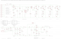
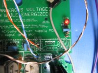
A/C voltage doubler section test
The voltage on the meter is unloaded. I'll scope it for ripple levels once the voltage regulator section is done and the doubler is loaded. A 24Vac transformer is being used.
I've decided to bleed the thing down a bit faster when the power is off, so the bleeders are reduced to 10K on the next board turn, which means they go up to 1/4W. I'm also going to use that "free" current flow through the bleeders to power a couple of 3mm LEDs to give an indication when the power switch is on. The recitifier diodes are increasing to 2A to make it more useful for some other higher-current applications I have in mind. 🙂
Attachments


Last edited:
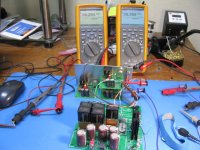
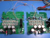
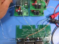
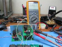
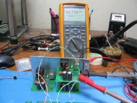
DC baseline measurements on batteries
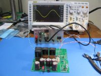
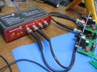
Here are a set of mesaurements to baseline the power supply board, powering a Victor oscillator with a simple battery supply, before using the current sources. Three of the battery positions have shorting snaps installed, leaving 4 x 9Vdc = 36Vdc. The board being powered is an 11KHz Victor oscillator.
* The first 3 photos just show the test setup. Those twisted pairs are just pulled out of some CAT5 ethernet cable.
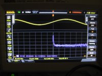
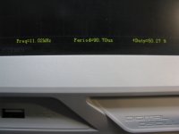
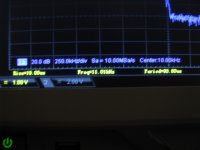
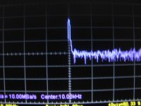
* The next photo shows what the scope comes up with for frequency and duty cycle. Of course this is only so accurate with a scope. The two digits past the decimal are bouncing around a bit on either side of 11.00KHz and 50.00% duty cycle.. The amplitude of Victor's board is set for 2Vp-p here.
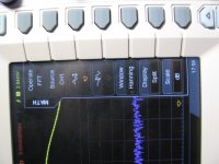
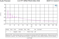
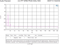
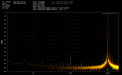
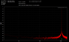
* The next 4 photos shows what the scope comes up with for an FFT, along with the FFT parameters. Sorry about the less-than-sharp photo, I had most of the lights off to reduce glare on the display. The "center" of 10KHz it shows is the center of the display area, not a calculated center of the (11KHz) fundamental. I should have done a close-up of the peak, but it is slightly to the right of center (1KHz worth) as expected. I've reduced the output of Victor's oscillator to 1V peak-to-peak for the FFT measurements.
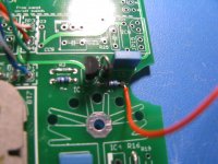
* The next photo is the current draw of Victor's board, about 29mA, but that is with essentially zero loading (1meg scope input).
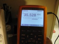
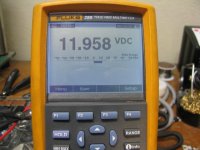
* And finally the exact measured voltage of the 4 batteries feeding Victor's board. Nearly spot-on with his recommended 35Vdc!
Here are a set of mesaurements to baseline the power supply board, powering a Victor oscillator with a simple battery supply, before using the current sources. Three of the battery positions have shorting snaps installed, leaving 4 x 9Vdc = 36Vdc. The board being powered is an 11KHz Victor oscillator.
* The first 3 photos just show the test setup. Those twisted pairs are just pulled out of some CAT5 ethernet cable.
* The next photo shows what the scope comes up with for frequency and duty cycle. Of course this is only so accurate with a scope. The two digits past the decimal are bouncing around a bit on either side of 11.00KHz and 50.00% duty cycle.. The amplitude of Victor's board is set for 2Vp-p here.
* The next 4 photos shows what the scope comes up with for an FFT, along with the FFT parameters. Sorry about the less-than-sharp photo, I had most of the lights off to reduce glare on the display. The "center" of 10KHz it shows is the center of the display area, not a calculated center of the (11KHz) fundamental. I should have done a close-up of the peak, but it is slightly to the right of center (1KHz worth) as expected. I've reduced the output of Victor's oscillator to 1V peak-to-peak for the FFT measurements.
* The next photo is the current draw of Victor's board, about 29mA, but that is with essentially zero loading (1meg scope input).
* And finally the exact measured voltage of the 4 batteries feeding Victor's board. Nearly spot-on with his recommended 35Vdc!
Attachments
-
 IMG_3514.JPG115.5 KB · Views: 131
 -
 IMG_3507.JPG156.6 KB · Views: 128
 -
 IMG_3506.JPG144.4 KB · Views: 115
 -
 IMG_3504.JPG123.6 KB · Views: 115
 -
 IMG_3503.JPG108.1 KB · Views: 140
 -
 IMG_3500.JPG148.5 KB · Views: 145
 -
 IMG_3499.JPG109.7 KB · Views: 133
 -
 IMG_3496.JPG166.2 KB · Views: 141
 -
 IMG_3495.JPG185.7 KB · Views: 164
 -
 IMG_3494.JPG179.1 KB · Views: 167
Last edited:
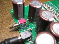
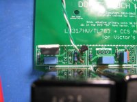
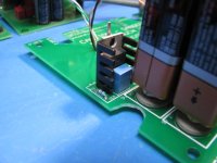
Walt Jung's current source article fig 13C no longer works! DN2540 has changed.
WOW, here is a discovery. I couldn't get the per-Victor-board current sources on this power supply board to work at all, with the circuit being taken directly from figure 13C in Walt Jung's excellent old "current sources for audio" paper here
waltjung.org/PDFs/Sources_101_P2.pdf
with the DN2540 depletion mosfet cascoding a LM317 wired as a current source. After a couple of hours troubleshooting the problem it turns out that the properties of the DN2540 have apparently changed since Walt wrote that article in 2007. At that time the Vgs of the part was apparently around -2.25V, which as Walt notes was already on the small side for voltage drop across a LM317, putting it in a "grey area" operationally as he wrote. But iit worked, and that is why he said the circuit was good up to only 38mA. The Vgs past that point would get too small for the LM317. In figure 12A of Walt's paper he shows 30mA output for a DN2540 with a 75R set resistor, which would be a Vgs of 75 * 30mA = 2.25Vdc.
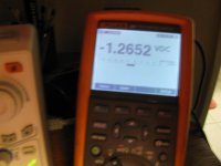
Well now I'm measuring -1.26V for Vgs at 35mA on the current crop of DN2540s, as shown in the photo below! This is a brand new part from Newark/Element14. Good grief. I've tried two of them from the same antistat bag with the same result. That of course is way too little voltage drop across a LM317 to even turn it on, which is what was happening. At first I thought there must be something different about the to-92 LM317L vs. the to-220 LM317 and tack soldered a LM317 in instead. Nothing. Then measured the voltages and found this problem.
The company that makes the DN2540 used to be Supertex but was recently sold to Microchip Tech. Maybe Microchip is the one who messed with the part. At any rate 1.26V just isn't going to work across a LM317. That circuit Walt published in 13C with the DN2540 cascoding a LM317 is simply not going to work anymore.
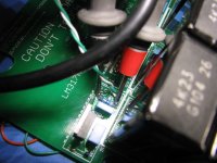
In the photos below I re-wired things with jumper wires on the back of the PCB to only use the DN2540 as the current source (figure 12A in Walt's paper), leaving the LM317 out entirely. That works great as the photos show. There may be a way to "fix" the original circuit for low d-mosfet Vgs by inserting a zener or LED between the mosfet source and LM317 input to bump the voltage across the LM317 back up to something reasonable.
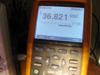
* The first 5 photos are the "rewired" circuit of just a DN2540 d-mosfet current source set for 35mA. Results in the 36.8Vdc measured across a Victor oscillator board. I reduced the number of batteries to 5 for this test to keep the dissipation in the DN2540 down. With 7 batteries it is pushing about a watt and would need a heatsink attached, which I've left space for. 5 batteries dissipates only about 1/2W.
* The next two photos are the Vgs measured across a 36 ohm d-mosfet current source "set" resistor: 1.26Vdc, miles away from the 2.25Vdc the part had in Walt's article back in 2007.
WOW, here is a discovery. I couldn't get the per-Victor-board current sources on this power supply board to work at all, with the circuit being taken directly from figure 13C in Walt Jung's excellent old "current sources for audio" paper here
waltjung.org/PDFs/Sources_101_P2.pdf
with the DN2540 depletion mosfet cascoding a LM317 wired as a current source. After a couple of hours troubleshooting the problem it turns out that the properties of the DN2540 have apparently changed since Walt wrote that article in 2007. At that time the Vgs of the part was apparently around -2.25V, which as Walt notes was already on the small side for voltage drop across a LM317, putting it in a "grey area" operationally as he wrote. But iit worked, and that is why he said the circuit was good up to only 38mA. The Vgs past that point would get too small for the LM317. In figure 12A of Walt's paper he shows 30mA output for a DN2540 with a 75R set resistor, which would be a Vgs of 75 * 30mA = 2.25Vdc.
Well now I'm measuring -1.26V for Vgs at 35mA on the current crop of DN2540s, as shown in the photo below! This is a brand new part from Newark/Element14. Good grief. I've tried two of them from the same antistat bag with the same result. That of course is way too little voltage drop across a LM317 to even turn it on, which is what was happening. At first I thought there must be something different about the to-92 LM317L vs. the to-220 LM317 and tack soldered a LM317 in instead. Nothing. Then measured the voltages and found this problem.
The company that makes the DN2540 used to be Supertex but was recently sold to Microchip Tech. Maybe Microchip is the one who messed with the part. At any rate 1.26V just isn't going to work across a LM317. That circuit Walt published in 13C with the DN2540 cascoding a LM317 is simply not going to work anymore.
In the photos below I re-wired things with jumper wires on the back of the PCB to only use the DN2540 as the current source (figure 12A in Walt's paper), leaving the LM317 out entirely. That works great as the photos show. There may be a way to "fix" the original circuit for low d-mosfet Vgs by inserting a zener or LED between the mosfet source and LM317 input to bump the voltage across the LM317 back up to something reasonable.
* The first 5 photos are the "rewired" circuit of just a DN2540 d-mosfet current source set for 35mA. Results in the 36.8Vdc measured across a Victor oscillator board. I reduced the number of batteries to 5 for this test to keep the dissipation in the DN2540 down. With 7 batteries it is pushing about a watt and would need a heatsink attached, which I've left space for. 5 batteries dissipates only about 1/2W.
* The next two photos are the Vgs measured across a 36 ohm d-mosfet current source "set" resistor: 1.26Vdc, miles away from the 2.25Vdc the part had in Walt's article back in 2007.
Attachments
Last edited:
Characteristics of depletion MOSFETs and JFETs vary all over the lot. That's why I sell the Impasse printed circuit boards with the source resistors adjusted so that each channel matches.
LM317 is probably not an ideal regulator in this application. The error amp is such that it puts harmonics back onto the power supply rail. Furthermore, battery noise is measured in picoVolts per root Hertz, the LM317 noise, even with the adjust pin decoupled, is 100's of nanoVolts per root Hertz.
LM317 is probably not an ideal regulator in this application. The error amp is such that it puts harmonics back onto the power supply rail. Furthermore, battery noise is measured in picoVolts per root Hertz, the LM317 noise, even with the adjust pin decoupled, is 100's of nanoVolts per root Hertz.
First is an FFT of the LM317, bypassed adjust pin with a small 1kHz tone put on the positive rail. The regulator puts its own harmonic imprint onto the power supply rail. Second is the Jung regulator which deals much more effectively.
This analysis came about from one of the readers of the Linear Audio article on power supply regulators.
This analysis came about from one of the readers of the Linear Audio article on power supply regulators.
Attachments
jackinnj - very interesting plots, thanks! 🙂 I agree, it does look like the LM317 would heap noise on top of the othewise-quiet battery supply. That is one of the reasons I've put both batteries and an AC supply on the board as modular sections, plus made things like the per-board CCS modular. Makes it easy to A/B various configurations: AC vs. batteries (the results of the output spectrum from Victor's boards) and A/B things like batteries direct vs. going through the per-board CCS.
luvdunhill - good thoughts, I've been pondering that! Using an LDO would solve the less-than-1.26Vdc problem and possibly be less noisy, if something newer like the LT3080 with a feedforward cap was used. The trick is the ground line on LDOs vs. the 317 being floating, given the setup on Victor's boards with the TL431's and system ground tied in the middle. If a cascoded LDO was used it might be "safer" in terms of avoiding ground loops to use it as a current sink rather than source, so the LDO ground line and "set" resistor coming off the source would both be tied to the power supply ground.
BUT...some good news...looks like a little forum searching would have saved me some time. 🙂 I've found this forum thread on Walt's circuit, specifically that fig 13C DN2540 + LM317 cascode:
http://www.diyaudio.com/forums/tubes-valves/189735-dn2540-lm317-cascode-ccs.html
and in there SY's post #2 about Walt Jung posting a follow-up in 2009 as a letter to the editor:
http://www.waltjung.org/PDFs/Sources_101_Letter_Revisit_0409.pdf (from Walt's site, opens a PDF)
where he notes that just using one DN2540 to cascode another beats the DN2540 + LM317 cascode by quite a bit. The circuit is in figure 1 in that link and the AP measurements in figure 2. -150dB up to 1KHz, then rises to -130dB at 20KHz. Good enough! 😀 I think I knew about that letter to the editor at one time then forgot about it.
The big attraction for me with Walt's double-DN2540 CCS is that it has been measured. A cascoded LDO would be (a lot) more accurate, and possibly quiester, but without an AP measurement with a specific LDO for proof I think that I'm going to go with the known quantity for now.
So I've re-designed the per-Victor board CCS row on the power supply board this evening to use the 2 DN2540 CCS cascode for the next V2.0, layout so far below. The cascode DN2540 is still the TO-220 version since it gets all the voltage (and dissipation), while the cascoded one is the TO-92 N3 version. So the whole thing actually looks a lot like the previous layout, since the LM317 was the TO-92 version.
In fact, it's so similar I was able to just turn a TO-92 DN2540 90 degrees, stick it in the same PCB holes for the LM317, then cut one trace underneathg and solder in a 1K gate stopper. Then change the other gate stopper to 1K from 100R (a suggestion I've picked up in the reading). Just like that in the photos below I have the circuit working to test with. 🙂 DC tests for now, I'l take a look with the scope and eventually the Victor board output with the QA-400 later in the week.
To deal with the DN2540 Vgs varying from batch to batch I've put a 1/4W sized "set" resistor pad (2.29mm diameter, 6.1mm long through hole) in series with a 1/8W sized pad (1.5mm diameter, 3.5mm long). The two can be mixed and matched to come up with whatever value is required after measuring the actual Vgs (Vgs /35mA = Rset of course), relative to whatever Mouser / Digikey have in stock at the moment. For the test circuit here I used a 36R 1/8W 1% metal film I had on hand, but I have a bunch of 35.7R's arriving from Mouser tomorrow since that turned out to be a common value. On the new V2.0 board then I would have just jumpered over the 1/4W resistor position.
I thought of using a trimpot in series with the set resistor, but since the result is current and not voltage it probably wouldn't help. The DN2540 Vgs would still have to be measured, then the trimpot set with an ohmmeter before inserting. Might as well just use the fixed resistors, it seems.
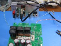
I also built up the low battery comparator's LR12 12V power supply and that works, photos below.
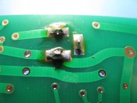
* The first two photos show the surgery to convert one per-board-CCS section from DN2540 + LM317 to TO-220 DN2540 cascoding a TO-92 DN2540.
* The next photo shows the result with the 35mA CCS feeding a Victor oscillator, 39.2Vdc at the board terminals with zero load on the board.
* The next three photos are the 12V LR12 power supply section for the low-battery comparator and the unloaded voltage result.
* V2.0 print and layout so far. I'm going to try for plated slots on the power jack this time rather than holes, thanks to some help from CADsoft. It will be interesting to see if they come out properly. The batteries are all 0.6mm closer to each other, to make the whole stack solid enough to put a band around if someone wants to mechanically stabilize them some more. The end mount battery snaps have really tight grip though, just by themselves.
luvdunhill - good thoughts, I've been pondering that! Using an LDO would solve the less-than-1.26Vdc problem and possibly be less noisy, if something newer like the LT3080 with a feedforward cap was used. The trick is the ground line on LDOs vs. the 317 being floating, given the setup on Victor's boards with the TL431's and system ground tied in the middle. If a cascoded LDO was used it might be "safer" in terms of avoiding ground loops to use it as a current sink rather than source, so the LDO ground line and "set" resistor coming off the source would both be tied to the power supply ground.
BUT...some good news...looks like a little forum searching would have saved me some time. 🙂 I've found this forum thread on Walt's circuit, specifically that fig 13C DN2540 + LM317 cascode:
http://www.diyaudio.com/forums/tubes-valves/189735-dn2540-lm317-cascode-ccs.html
and in there SY's post #2 about Walt Jung posting a follow-up in 2009 as a letter to the editor:
http://www.waltjung.org/PDFs/Sources_101_Letter_Revisit_0409.pdf (from Walt's site, opens a PDF)
where he notes that just using one DN2540 to cascode another beats the DN2540 + LM317 cascode by quite a bit. The circuit is in figure 1 in that link and the AP measurements in figure 2. -150dB up to 1KHz, then rises to -130dB at 20KHz. Good enough! 😀 I think I knew about that letter to the editor at one time then forgot about it.
The big attraction for me with Walt's double-DN2540 CCS is that it has been measured. A cascoded LDO would be (a lot) more accurate, and possibly quiester, but without an AP measurement with a specific LDO for proof I think that I'm going to go with the known quantity for now.
So I've re-designed the per-Victor board CCS row on the power supply board this evening to use the 2 DN2540 CCS cascode for the next V2.0, layout so far below. The cascode DN2540 is still the TO-220 version since it gets all the voltage (and dissipation), while the cascoded one is the TO-92 N3 version. So the whole thing actually looks a lot like the previous layout, since the LM317 was the TO-92 version.
In fact, it's so similar I was able to just turn a TO-92 DN2540 90 degrees, stick it in the same PCB holes for the LM317, then cut one trace underneathg and solder in a 1K gate stopper. Then change the other gate stopper to 1K from 100R (a suggestion I've picked up in the reading). Just like that in the photos below I have the circuit working to test with. 🙂 DC tests for now, I'l take a look with the scope and eventually the Victor board output with the QA-400 later in the week.
To deal with the DN2540 Vgs varying from batch to batch I've put a 1/4W sized "set" resistor pad (2.29mm diameter, 6.1mm long through hole) in series with a 1/8W sized pad (1.5mm diameter, 3.5mm long). The two can be mixed and matched to come up with whatever value is required after measuring the actual Vgs (Vgs /35mA = Rset of course), relative to whatever Mouser / Digikey have in stock at the moment. For the test circuit here I used a 36R 1/8W 1% metal film I had on hand, but I have a bunch of 35.7R's arriving from Mouser tomorrow since that turned out to be a common value. On the new V2.0 board then I would have just jumpered over the 1/4W resistor position.
I thought of using a trimpot in series with the set resistor, but since the result is current and not voltage it probably wouldn't help. The DN2540 Vgs would still have to be measured, then the trimpot set with an ohmmeter before inserting. Might as well just use the fixed resistors, it seems.
I also built up the low battery comparator's LR12 12V power supply and that works, photos below.
* The first two photos show the surgery to convert one per-board-CCS section from DN2540 + LM317 to TO-220 DN2540 cascoding a TO-92 DN2540.
* The next photo shows the result with the 35mA CCS feeding a Victor oscillator, 39.2Vdc at the board terminals with zero load on the board.
* The next three photos are the 12V LR12 power supply section for the low-battery comparator and the unloaded voltage result.
* V2.0 print and layout so far. I'm going to try for plated slots on the power jack this time rather than holes, thanks to some help from CADsoft. It will be interesting to see if they come out properly. The batteries are all 0.6mm closer to each other, to make the whole stack solid enough to put a band around if someone wants to mechanically stabilize them some more. The end mount battery snaps have really tight grip though, just by themselves.
Attachments
-
 IMG_3528.JPG54.2 KB · Views: 113
 -
 IMG_3527.JPG66 KB · Views: 116
 -
 IMG_3526.JPG71.8 KB · Views: 124
 -
 IMG_3529.JPG70 KB · Views: 113
 -
 IMG_3532.JPG41.4 KB · Views: 112
 -
 IMG_3530.JPG62.8 KB · Views: 177
 -
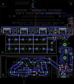
layout.pdf92.5 KB · Views: 55
-
 layout.jpg726.7 KB · Views: 103
 -
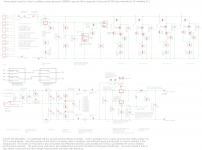
schematic.pdf41.3 KB · Views: 110
-
 schematic.png110 KB · Views: 152
Last edited:
Current sources now sinks
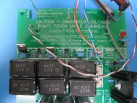
Thinking about the graphs in jackinnj's posts a bit more I've decided to run the cascoded dual DN2540 constant current sources as current sinks rather than sources. Just as with the AC from the load getting into the LM317's adjust pin in jackinnj's graphs there would be a similar chance of load noise making it into the "set" DN2540's gate when run as a source. When run as a sink all the load sees is the drain of the cascode DN2540.
I've reworked the layout as such and did more cut-and-jumpering on the existing board in the photos to test the current sink arrangement. So far these are just DC tests. I've built up a second per-board CCS section to power the 10KHz Victor oscillator along with the 11KHz, looking for any potential interaction with the shared ground in the middle of the board's TL431's.
I've built up the main voltage regulator section and the low battery circuit and they both work. In the photos below I have one with 5 batteries where the red low battery LED is on, then another with six batteries where it is off. The voltage across the two Victor board power inputs from the current feeds is steady going between 5 and 6 batteries, as the meter readings in the photos show.
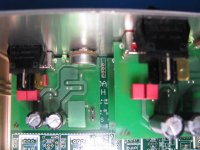
* The first photo shows the test setup. Each meter is on the power input of a different Victor oscillator. 5 batteries in use at this point, so the low battery LED set for 46Vdc is on. Hard to see in this photo, but I have a better one below.
* The next two photos show the cut and jumper to convert the leftmost two per-board CCS sections into current sinks. The trace feeding the cascode drain is cut, then the board feed wires soldered on either side.
* The next photo shows a closeup of the low battery light on with the 5 batteries. The surface mount comparator chip is just below the LED. The holes where the LED is are intended to wire out to a panel LED. Those same traces go to the holes for the dual stack front panel LED on the board.
* The next photo shows the completed voltage regulator section with the LM317HV installed in the on-board heatsink position rather than the rear panel heatsink holes. Works great, although I didn't take a picture of the Vout here. One change for V3.0 is that I used the wrong heat sink outline on the silk screen. Luckily for testing the smaller one has the same mounting holes as that larger unit.
* The next one shows 6 batteries installed with the low battery light now off. Works great. 🙂
* This photo shows the meter readings with 6 batteries installed. 39.295Vdc for the 11KHz Victor board, vs. 39.311Vdc with 5 batteries. 39.569Vdc for the 10KHz board with 6 batteries vs. 39.589 with 5 batteries.
* The final shot shows how a heatsink fits in around the TO-220 DN2540. This was just a PC mount heat sink I grabbed quickly.
Thinking about the graphs in jackinnj's posts a bit more I've decided to run the cascoded dual DN2540 constant current sources as current sinks rather than sources. Just as with the AC from the load getting into the LM317's adjust pin in jackinnj's graphs there would be a similar chance of load noise making it into the "set" DN2540's gate when run as a source. When run as a sink all the load sees is the drain of the cascode DN2540.
I've reworked the layout as such and did more cut-and-jumpering on the existing board in the photos to test the current sink arrangement. So far these are just DC tests. I've built up a second per-board CCS section to power the 10KHz Victor oscillator along with the 11KHz, looking for any potential interaction with the shared ground in the middle of the board's TL431's.
I've built up the main voltage regulator section and the low battery circuit and they both work. In the photos below I have one with 5 batteries where the red low battery LED is on, then another with six batteries where it is off. The voltage across the two Victor board power inputs from the current feeds is steady going between 5 and 6 batteries, as the meter readings in the photos show.
* The first photo shows the test setup. Each meter is on the power input of a different Victor oscillator. 5 batteries in use at this point, so the low battery LED set for 46Vdc is on. Hard to see in this photo, but I have a better one below.
* The next two photos show the cut and jumper to convert the leftmost two per-board CCS sections into current sinks. The trace feeding the cascode drain is cut, then the board feed wires soldered on either side.
* The next photo shows a closeup of the low battery light on with the 5 batteries. The surface mount comparator chip is just below the LED. The holes where the LED is are intended to wire out to a panel LED. Those same traces go to the holes for the dual stack front panel LED on the board.
* The next photo shows the completed voltage regulator section with the LM317HV installed in the on-board heatsink position rather than the rear panel heatsink holes. Works great, although I didn't take a picture of the Vout here. One change for V3.0 is that I used the wrong heat sink outline on the silk screen. Luckily for testing the smaller one has the same mounting holes as that larger unit.
* The next one shows 6 batteries installed with the low battery light now off. Works great. 🙂
* This photo shows the meter readings with 6 batteries installed. 39.295Vdc for the 11KHz Victor board, vs. 39.311Vdc with 5 batteries. 39.569Vdc for the 10KHz board with 6 batteries vs. 39.589 with 5 batteries.
* The final shot shows how a heatsink fits in around the TO-220 DN2540. This was just a PC mount heat sink I grabbed quickly.
Attachments
-
 IMG_3545.JPG50.6 KB · Views: 108
 -
 IMG_3542.JPG76.1 KB · Views: 104
 -
 IMG_3541.JPG62.9 KB · Views: 99
 -
 IMG_3538.JPG71.2 KB · Views: 97
 -
 IMG_3537.JPG81.7 KB · Views: 98
 -
 IMG_3546.JPG49.6 KB · Views: 96
 -
 IMG_3536.JPG63.4 KB · Views: 111
 -
 IMG_3533.JPG82.2 KB · Views: 142
 -
 schematic.png110.7 KB · Views: 126
 -
 layout.jpg723.6 KB · Views: 108
Last edited:
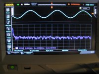
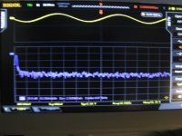
THD+N measurements
Here are the THD+N plots done using a QA400. I've run them both with the Victor 10KHz and 11KHz oscillators powered by batteries and through the per-board current sinks on the power supply board, then again using the AC voltage doubler feeding the 48Vdc regulator and then into the per-board current sinks. The plots look identical in terms of a complete absence of any 60Hz or powerline harmonics above the background EMI from the room flluorescent lights (that show with the battery-operated plot).
So the bottom line: within the measuring capability of the QA400 the AC power supply on this board appears to be as good as batteries for powering Victor's oscillators. I would expect that an AP or dSccope would most likely find additional noise though in the next decade or two down past what the QA400 can do.
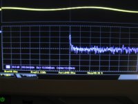
One interesting thing that did pop up is what appears to be IMD when both the 10KHZ and 11KHz signals are being applied, if I'm looking at that right. In the plots below with both the 10KHZ and 11KHZ signals fed in via the left and right channels I'm seeing 1Khz (difference frequency), 2KHz, 3KHz, etc. Happens with either batteries or AC. There is the chance is could somehow be a result the common ground connection between the two Victor boards. I'm still thinking about a way to isolate whether this is a (dual) Victor ocillator issue or an issue of IMD inside the QA400. Maybe unbolt one oscillator from the front panel and power it with separate batteries. Lol, I'm out of my depth here. Hopefully someone who knows a lot more about this stuff than me can comment.
* First three plots are the 10KHz Victor board into the QA400 right channel, 11KHz into the left channel, then both at the same time. All using batteries powering the per-board current drains on power board.
* Next three plots are the 10KHz Victor board into the QA400 right channel, 11KHz into the left channel, then both at the same time. All using The AC voltage doubler into the 48Vdc voltage regulator, powering the per-board current drains on the power board.
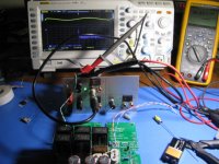
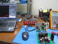
* Next two photos are the test setup with the QA400. This is running on AC. It is almost cut off in the photo but a 24Vac power adaptor is plugged into the power jack at the bottom of the board. I've left the batteries in here, but that blue and white wire pair to the left of the board that is unhooked is the output of the batteries. Here the output of the 48Vdc on-board voltage regulator (the large heat sink) is powering the per-board current sinks. The DMM is on the output of the voltage regulator.
* Next two photos are a scope FFT of the 10KHz oscillator and the 11KHz. These are done with both Victor boards (10KHz, 11Khz) connected to scope channels at the same time, so the boards' signal grounds would be tied together.
Here are the THD+N plots done using a QA400. I've run them both with the Victor 10KHz and 11KHz oscillators powered by batteries and through the per-board current sinks on the power supply board, then again using the AC voltage doubler feeding the 48Vdc regulator and then into the per-board current sinks. The plots look identical in terms of a complete absence of any 60Hz or powerline harmonics above the background EMI from the room flluorescent lights (that show with the battery-operated plot).
So the bottom line: within the measuring capability of the QA400 the AC power supply on this board appears to be as good as batteries for powering Victor's oscillators. I would expect that an AP or dSccope would most likely find additional noise though in the next decade or two down past what the QA400 can do.
One interesting thing that did pop up is what appears to be IMD when both the 10KHZ and 11KHz signals are being applied, if I'm looking at that right. In the plots below with both the 10KHZ and 11KHZ signals fed in via the left and right channels I'm seeing 1Khz (difference frequency), 2KHz, 3KHz, etc. Happens with either batteries or AC. There is the chance is could somehow be a result the common ground connection between the two Victor boards. I'm still thinking about a way to isolate whether this is a (dual) Victor ocillator issue or an issue of IMD inside the QA400. Maybe unbolt one oscillator from the front panel and power it with separate batteries. Lol, I'm out of my depth here. Hopefully someone who knows a lot more about this stuff than me can comment.
* First three plots are the 10KHz Victor board into the QA400 right channel, 11KHz into the left channel, then both at the same time. All using batteries powering the per-board current drains on power board.
* Next three plots are the 10KHz Victor board into the QA400 right channel, 11KHz into the left channel, then both at the same time. All using The AC voltage doubler into the 48Vdc voltage regulator, powering the per-board current drains on the power board.
* Next two photos are the test setup with the QA400. This is running on AC. It is almost cut off in the photo but a 24Vac power adaptor is plugged into the power jack at the bottom of the board. I've left the batteries in here, but that blue and white wire pair to the left of the board that is unhooked is the output of the batteries. Here the output of the 48Vdc on-board voltage regulator (the large heat sink) is powering the per-board current sinks. The DMM is on the output of the voltage regulator.
* Next two photos are a scope FFT of the 10KHz oscillator and the 11KHz. These are done with both Victor boards (10KHz, 11Khz) connected to scope channels at the same time, so the boards' signal grounds would be tied together.
Attachments
-
 IMG_3554.JPG58.5 KB · Views: 183
 -
 IMG_3553.JPG57.9 KB · Views: 237
 -
 IMG_3577.JPG78.9 KB · Views: 234
 -
 IMG_3576.JPG76.8 KB · Views: 214
 -
 On AC power - 10KHz & 11KHz boards connected.png59.8 KB · Views: 168
 -
 On AC power - only 11KHz board connected.png42.4 KB · Views: 408
 -
 On AC power - only 10KHz board connected.png43.2 KB · Views: 393
 -
 On battery power - 10KHz & 11KHz boards connected.png59.5 KB · Views: 397
 -
 On battery power - only 11KHz board connected.png42.6 KB · Views: 415
 -
 On battery power - only 10KHz board connected.png42.9 KB · Views: 415
Last edited:
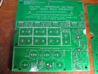
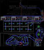
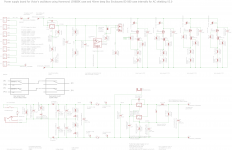
V3.0 is back - Gerbers! Plus optionally using 2 cases.
V 3.0 of the Victor oscillator power board came back from fabrication yesterday and fits/works perfectly! So Gerber files are posted below plus a text file with instructions to give the fab house, if anyone wants to make one of these boards,
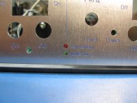
Everything fit mechanically just perfectly this time, as the photos show. 🙂 The two side notches for the Hammond case are in exactly the right place, as are the two front notches for the ground bolts on the lower two Victor boards. Even the front panel LED stack is centered properly this time. My attempt at using 3 slots for the 2.1mm/5.5mm barrel power jack instead of 3 holes even worked. Now that alone deserves a beer! Lol, I've been trying for months to find a way to get Eagle to do slots.
As expected the Vgs of the DN2540 mosfets is all over the place. With this dual DN2540 cascode current sink arrangement you will have to start with a "guess" set resistor, like 62 ohms, then measure the Vgs on each of the per-board current sinks, do the math (Vgs / 0.25 = resistor) and replace that 62 ohm with the correct thing to give you exactly 25mA. I built up 3 CCS sections on this first test V3.0 board. One CCS section had a measured Vgs of 1.62V, another 1.58V, and the third 1.47V. Last time, with the V2.0 board, I was getting 1.26V for all three in the lot.
Which is another thing - I had a bit of a brain hiccup going on the last board's CCS set resistor calculations. I don't know why I started using 35mA instead of 25mA, Victor's board uses 25mA. 35V input as specified by Victor, minus the 30V formed across the current shunts, leaves 5V accross the 2 100R restors. 5V / 200R = 25mA. I'll revise the BOM and schematic labelling accordingly. 35mA used for an extended period of time would likely fry the TL431 current shunts on Victor's boards.
I want to mention one other slick thing you can do here. There is nothing that would prevent using this Victor oscillator power board in its own Hammond 1598EBK case. So one 1598EBK just for the Victor oscillators using the front panels I've already posted here, then a second 1598EBK for the power board. The benefit in doing so is completely removing any power supply heat generation from the oscillator box with Victor's boards. The concern here is small amounts of thermal drift in Victor's oscillators over time if the inside of the case heats up. I have things set up so that the LM317HV can be heat sinked to the rear panel, which will help, but still some heat from that will radiate into the box. The per-board current sinks also dissipate a bit of heat. I'm going to put lots of ventilation slots in the rear panel (CAD file to be posted!) that has the two power switches.
Using one case for the power board and another just for the oscillators is especially slick if you use ethernet cable to hook them together! I'm already using CAT 5 twisted ethernet pairs as the hookup wire between sections. Since there are (up to) 4 Victor ocillators on the front panel, (up to) 4 per-board CCS sections on the power supply, and 4 pairs in a CAT 5 cable, you can just use RJ45 jacks to connect the power between the two cases. Use one RJ45 on the front panel of the power supply-only 1598EBK case, another RJ45 on the rear panel of the Victor oscillator-only 1598EBK case, and then use an off-the-shelf CAT 5 patch cable to connect the two. The various specifications I've found for RJ45 current handling range between 0.5A and 1.2A per contact. Here they will only have to carry 0.025A per contact, the amount for one Victor board.
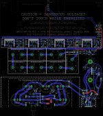
In the photos below:
* 3588 and 3589 show the V3.0 board fits perfectly in the Hammond 1598EBK case now, including around the two side supports.
* 3590 & 3591 show the V3.0 board clears the two Victor board ground studs on the bottom boards now, and the stacked indicator LED is centered this time.
* 3592, 3594 & 3595 show the power jack slots!!
* 3600 shows the pervious V2.0 board on the left, and a built-up V3.0 board on the right. The board shade of green changed slightly because I went with a different fab house this time.
V 3.0 of the Victor oscillator power board came back from fabrication yesterday and fits/works perfectly! So Gerber files are posted below plus a text file with instructions to give the fab house, if anyone wants to make one of these boards,
Everything fit mechanically just perfectly this time, as the photos show. 🙂 The two side notches for the Hammond case are in exactly the right place, as are the two front notches for the ground bolts on the lower two Victor boards. Even the front panel LED stack is centered properly this time. My attempt at using 3 slots for the 2.1mm/5.5mm barrel power jack instead of 3 holes even worked. Now that alone deserves a beer!
Lol, I've been trying for months to find a way to get Eagle to do slots.As expected the Vgs of the DN2540 mosfets is all over the place. With this dual DN2540 cascode current sink arrangement you will have to start with a "guess" set resistor, like 62 ohms, then measure the Vgs on each of the per-board current sinks, do the math (Vgs / 0.25 = resistor) and replace that 62 ohm with the correct thing to give you exactly 25mA. I built up 3 CCS sections on this first test V3.0 board. One CCS section had a measured Vgs of 1.62V, another 1.58V, and the third 1.47V. Last time, with the V2.0 board, I was getting 1.26V for all three in the lot.
Which is another thing - I had a bit of a brain hiccup going on the last board's CCS set resistor calculations. I don't know why I started using 35mA instead of 25mA, Victor's board uses 25mA. 35V input as specified by Victor, minus the 30V formed across the current shunts, leaves 5V accross the 2 100R restors. 5V / 200R = 25mA. I'll revise the BOM and schematic labelling accordingly. 35mA used for an extended period of time would likely fry the TL431 current shunts on Victor's boards.
I want to mention one other slick thing you can do here. There is nothing that would prevent using this Victor oscillator power board in its own Hammond 1598EBK case. So one 1598EBK just for the Victor oscillators using the front panels I've already posted here, then a second 1598EBK for the power board. The benefit in doing so is completely removing any power supply heat generation from the oscillator box with Victor's boards. The concern here is small amounts of thermal drift in Victor's oscillators over time if the inside of the case heats up. I have things set up so that the LM317HV can be heat sinked to the rear panel, which will help, but still some heat from that will radiate into the box. The per-board current sinks also dissipate a bit of heat. I'm going to put lots of ventilation slots in the rear panel (CAD file to be posted!) that has the two power switches.
Using one case for the power board and another just for the oscillators is especially slick if you use ethernet cable to hook them together! I'm already using CAT 5 twisted ethernet pairs as the hookup wire between sections. Since there are (up to) 4 Victor ocillators on the front panel, (up to) 4 per-board CCS sections on the power supply, and 4 pairs in a CAT 5 cable, you can just use RJ45 jacks to connect the power between the two cases. Use one RJ45 on the front panel of the power supply-only 1598EBK case, another RJ45 on the rear panel of the Victor oscillator-only 1598EBK case, and then use an off-the-shelf CAT 5 patch cable to connect the two. The various specifications I've found for RJ45 current handling range between 0.5A and 1.2A per contact. Here they will only have to carry 0.025A per contact, the amount for one Victor board.
In the photos below:
* 3588 and 3589 show the V3.0 board fits perfectly in the Hammond 1598EBK case now, including around the two side supports.
* 3590 & 3591 show the V3.0 board clears the two Victor board ground studs on the bottom boards now, and the stacked indicator LED is centered this time.
* 3592, 3594 & 3595 show the power jack slots!!
* 3600 shows the pervious V2.0 board on the left, and a built-up V3.0 board on the right. The board shade of green changed slightly because I went with a different fab house this time.
Attachments
-
 IMG_3595.JPG66.2 KB · Views: 118
 -
 IMG_3600.JPG86.1 KB · Views: 159
 -
Victor osc power supply 9_2_2015 V3.0 182.zip439 KB · Views: 72
-
Fabrication instructions.txt528 bytes · Views: 74
-
 IMG_3594.JPG44.1 KB · Views: 126
 -
 IMG_3592.JPG46.5 KB · Views: 137
 -
 IMG_3591.JPG34.3 KB · Views: 131
 -
 IMG_3590.JPG59.9 KB · Views: 132
 -
 IMG_3589.JPG77.4 KB · Views: 140
 -
 IMG_3588.JPG88.2 KB · Views: 180
Last edited:
more V3.0 photos
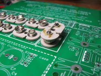
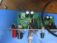
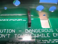
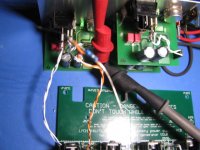
* 3602 shows the new dual cascoded DN2540 per-board constant current sink sections. I've attached heatsinks here with 3mm x 6mm long socket head bolts. I'll have the specifications in the BOM. The heatsink grease is just common GC type 44 zinc oxide.
* 3603 shows the new green "power on" LEDs, so I know when the AC switch is on now, lol. These are just in series with the bleeder resistors, so the current flow was already there to use. I've used T1 (3mm) diffused LEDs here. There is no requirement to have these LEDs - just jumper the positions across to get rid of them. That leaves the bleeder resistors in circuit, which are required. I just found it handy during testing to have some visual indication when the power switch was on! Those are 2 amp rectifier diodes now in V3.0, RL205's.
*3609 and 3611 show the voltage across the power input on one Victor board from a per-board CCS section, and the current, 34.8Vdc and 24.8mA. This is after one iteration of "meaure Vgs - swap CCS current set resistor - measure it all again"
* 3617 shows the wiring between the 3 per-board CCS sections and the 3 Victor oscillator boards.
Attachments

Last edited:
Revised front panels and front panel BOM
Here is a set of revised front panels for mounting Victor's oscillator boards, plus a revised BOM for the front panel parts involved.
What has changed from the previous panels:
* The lower boards in the 2, 3 and 4 board version for the Hammond 1598EBK case are moved up 2mm to provide a bit more clearance for the screw heads under the boards that mount the power board to the case.
* The two holes for the "power on" and "low battery" LEDs on the front of the V3.0 power board are added.
* For the 1-board version in the Box Enclosures B3-080 case, the Victor board is moved up 1mm.
* In the BOM I've added part numbers for the TE/Amp Faston quick disconnects that mate with the Carlon rocker switches, 0.187" x 0.032" variety.
Attachments
V3.1 Gerbers and BOM for the power supply board
The fabrication house made a mistake on my run of V3.0 boards that resulted in missing pads for the large heat sink. They re-did the board at their cost and were good enough to use a revised V3.1 set of Gerbers, posted below.
The changes are all cosmetic, no functionality differences:
* I've increased the size of some of the text on the board to be more readable.
* I've added 1mm to the lead spacing on the 1/4W sized resistors so that other, non-BOM types that are 7.3mm will fit well. Just increases the options for which parts can be used, in case the distributors are out of stock of a BOM resistor.
* I had forgotten to mark the polarity of the new LEDs in the AC doubler section. There is now a "long" to mark the long lead.
* Two resistors in the low-battery comparator section that were vertical are now horizontally mounted.
* I've added "(POS)" to one terminal of each set of twisted-pair PCB holes in each section to mark the positive lead.
* The spacing around the one large voltage regulator heat sink will now accomodate either the "thin" 12mm version or the "thick" 24mm version. Both are listed in the BOM. With the "thick" version on fin intrudes over the side notch for the case, but that doesn't matter since the large heat sink is not used with the case. If the board is used in the case use the rear-panel heat sink mounting position for the voltage regulator. The extruded heat sinks are just there if the board is being used as a table-top supply with the 4mm spacers for legs. The "thin" version of the heat sink will fit in the case, if someone should want the heat sink in the case.
I've added a "V3.1" folder to the Google Drive link in the first post of this thread, which has all the project materials.
I've designed the rear panel for the case now with the two switches, vent holes, power switch & power plug holes, and a hole for heat sinking the votlage regulator. The panel is in fabrication right now. Once I verify the holes line up I'll post the CAD file.
Attachments
Last edited:
beautiful work ! When I get back to USA in November, I will get back on this project.
THx-RNMarsh
THx-RNMarsh
Here is a set of revised front panels for mounting Victor's oscillator boards, plus a revised BOM for the front panel parts involved.
What has changed from the previous panels:
* The two holes for the "power on" and "low battery" LEDs on the front of the V3.0 power board are added.
* In the BOM I've added part numbers for the TE/Amp Faston quick disconnects that mate with the Carlon rocker switches, 0.187" x 0.032" variety.
I've just received a front panel back from Front Panel Express with the new CAD work. I'm happy to confirm the two LED holes line up just perfectly with the double-stack LED on the V3.1 power board. 😀
I'm also going to be posting a new version of the front panel BOM at the Google Drive link later today. One change. Turns out the insulated (crimp) Fastons stick out far enough that they don't really provide enough clearance to the two electrolytics on the back of Victor's board. The Fastons clear, but the wire coming out has to be bent at a sharp angle. To get the insulated Fastons on the rocker switch in the first place the switch has to be pushed out of the hole, then re-inserted.
The solution is to use un-insulated 0.187 x 0.032 inch Fastons, which is what I'm adding to the BOM. Just solder the wire on to the Faston. Plenty of room to insert the uninsulated version onto the switch tabs without takiing the rocker switch out of the panel. Plenty of room for the wire coming out of the back of the Faston to clear the caps. The 3rd photo below shows the uninsulated Fastsons being used.
Attachments
Last edited:
- Status
- Not open for further replies.
- Home
- Design & Build
- Equipment & Tools
- A case and power supply for Victor's low THD oscillators