You can already order from my webpage below. Look under DAC section at the end. There is a bit of lead time at this stage.
Relay is standard type, shunts and not in signal paths at all!
Controlled by a power monitoring chip on the underside. Also option for external control ...
Alternatively you can allways look here...perfect and simple solution....
Project 104 - Preamp/ crossover muting circuit

Project 104 - Preamp/ crossover muting circuit
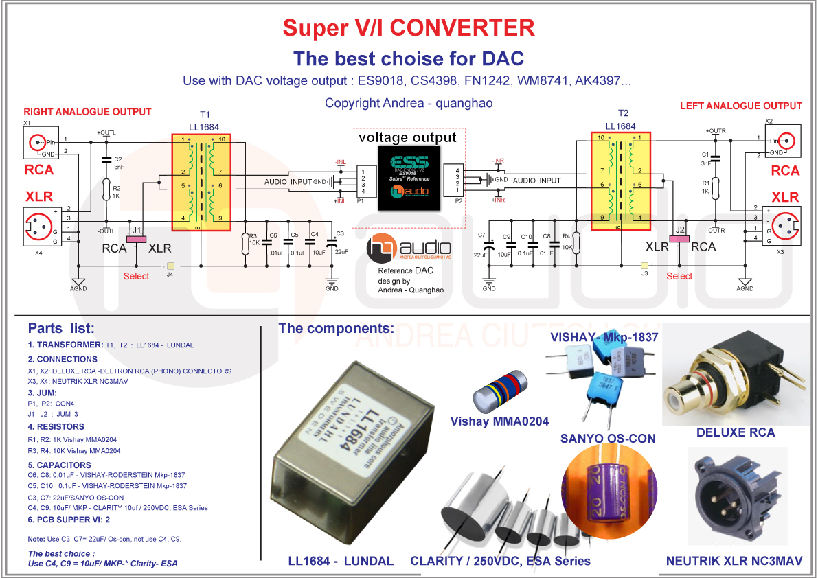
What about the Super V/I converted For DAC (http://www.diyaudio.com/forums/quanghao-audio-design/246579-super-v-i-converted-ll1684.html)?
Is it suitable for Soekris R2R?
This is completely unnecessary and essentially wrong approach here. As you could see this was designed for the ESS DAC which has balanced output with DC and something has to be between DAC and amp . The pure beauty of Soekirs's DAC is its simplicity. Driving straight from its RAW output is its main advantage. Just go by the rule - the less is more. If you have to, than jFet or tube buffer would be nice to isolate it from behind, but in most cases that is not even needed.
Acko's idea on transformer is quite valid and very interesting from a perspective of using Tr's natural roll off, but with that you are also introducing higher THD in lower part of the spectrum (with Lundahl 1674 that starts somewhere bellow 1 KHz and keeps rising as the Fq lowers) If transformer is introduced, one has to be very careful about its secondary loading and buffer there is even more recommended in order to make it independent from what amp / preamp is connected. I would think there is a clear advantage to having none, or just a buffer and not trying to complicate more or add something.
Modding the onboard buffers...
Probably not exactly what robert intended but I've replaced the LME49710 op-amps in the on-board buffer with LME49990's.
This was done at the same time as adding an 35V/56uF Panasonic FC electrolytic between the GND/Out pins on the ZLDO1117-33 regulator so can't say the improvement is entirely down to the upgraded op-amps.
It's possibly placebo but I think there is an improvement in transparency, sound staging and smoothness from the two mods. The LME49990 is an all round improvement in specs and has far better -Ve rail PSRR than the LME49710 which should help things along. The -Ve rail on the LME49710 is something like 20dB worse that the +Ve in terms of PSRR.
The LME49990's are cheap - the pair was under $10AU from Element14 - so worth trying out if you are using the onboard buffers.
I haven't been brave enough to try, but it looks like it might be possible to rework the output buffers so the LME49724 is wrapped in the LME49710/49990 feedback loop to form a composite amplifier. It would involve minor butchery of the PCB so hesitant to do so just yet.
I haven't been brave enough to try, but it looks like it might be possible to rework the output buffers so the LME49724 is wrapped in the LME49710/49990 feedback loop to form a composite amplifier. It would involve minor butchery of the PCB so hesitant to do so just yet.
Don't, the LME49724 is a real balanced amplifier, you can't just break one of its feedback loops....
Don't, the LME49724 is a real balanced amplifier, you can't just break one of its feedback loops....
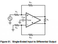
I was looking at working up something based on this:
Single-ended-to-differential converter has resistor-programmable gain | EDN
The idea is to wrap around the whole differential buffer with the feedback loops are left intact. Feedback for the first stage is taken from the negative output and feed that back to the +ve input of the LME49710/49990.
It needs some work in a simulator before I attempt hacking on the board.
That should be
got the + and - wrong way around.
Feedback for the first stage is taken from the +ve output and feed that back to the -ve input of the LME49710/49990.
got the + and - wrong way around.
Last edited:
Probably not exactly what robert intended but I've replaced the LME49710 op-amps in the on-board buffer with LME49990's.
This was done at the same time as adding an 35V/56uF Panasonic FC electrolytic between the GND/Out pins on the ZLDO1117-33 regulator so can't say the improvement is entirely down to the upgraded op-amps.
It's possibly placebo but I think there is an improvement in transparency, sound staging and smoothness from the two mods. The LME49990 is an all round improvement in specs and has far better -Ve rail PSRR than the LME49710 which should help things along. The -Ve rail on the LME49710 is something like 20dB worse that the +Ve in terms of PSRR.
The LME49990's are cheap - the pair was under $10AU from Element14 - so worth trying out if you are using the onboard buffers.
I haven't been brave enough to try, but it looks like it might be possible to rework the output buffers so the LME49724 is wrapped in the LME49710/49990 feedback loop to form a composite amplifier. It would involve minor butchery of the PCB so hesitant to do so just yet.
Paul, this is the kind of experimentation that I started the thread for. Whether folks prefer tubes, opamps, transformers, or transistors is up to personal taste, experience, resources, and implementation needs.
I will look forward to your review if the composite stage works out!
Paul, this is the kind of experimentation that I started the thread for. Whether folks prefer tubes, opamps, transformers, or transistors is up to personal taste, experience, resources, and implementation needs.
I will look forward to your review if the composite stage works out!
Just have to work up the courage to do the fine surgery involved. The circuit changes look like they can be done by cutting two traces and adding 3 short jumpers per channel. Trying to work out the best way to add required jumpers and it seems like adhesive copper tape might well be the best option...
There is a very old school article on the tape technique here:
http://www.hparchive.com/Bench_Briefs/HP-Bench-Briefs-1988-01-03.pdf
Aside from creating a composite stage there are two potential areas for improvement in the differential amp. The worst case CMRR of the LME49724 is determined by the matching of the gain resistors:
CMRR dB = 20log10(tolerance)
The stock board uses 0.5% tolerance resistors so:
CMRR db = 20log10(0.005)
= 46dB
This is well shy of the Datasheet spec of 102dB.
Improving the resistor tolerance to 0.1% increases the worst case CMRR to 60dB, and parts are reasonably obtainable and cheap.
Every additional improvement in tolerance gives roughly doubles the worst case CMRR, so that 0.05% = 66dB, 0.02% = 74dB, 0.01% = 80dB.
Once you go beyond 0.1% stocked values are pretty limited and you'd need to recalculate the gain resistors to use what is available.
The other possible improvement to the stock LME49724 config is adding a bypass cap to the Vocm pin. The datasheet suggests that noise on this pin reduces PSRR of the chip and recommends a 0.1-1uF cap in this position. There is potential that noise on the ground plane will have a negative impact on the PSSR, so adding a cap here may provide some benefit. I've got a couple of bags of 0.1uf MLCC ceramics around somewhere so I'll give this one a try and see if it helps at all.
Last edited:
Aside from creating a composite stage there are two potential areas for improvement in the differential amp. The worst case CMRR of the LME49724 is determined by the matching of the gain resistors:
CMRR dB = 20log10(tolerance)
The stock board uses 0.5% tolerance resistors so:
CMRR db = 20log10(0.005)
= 46dB
This is well shy of the Datasheet spec of 102dB.
Improving the resistor tolerance to 0.1% increases the worst case CMRR to 60dB, and parts are reasonably obtainable and cheap.
Every additional improvement in tolerance gives roughly doubles the worst case CMRR, so that 0.05% = 66dB, 0.02% = 74dB, 0.01% = 80dB.
Once you go beyond 0.1% stocked values are pretty limited and you'd need to recalculate the gain resistors to use what is available.
The other possible improvement to the stock LME49724 config is adding a bypass cap to the Vocm pin. The datasheet suggests that noise on this pin reduces PSRR of the chip and recommends a 0.1-1uF cap in this position. There is potential that noise on the ground plane will have a negative impact on the PSSR, so adding a cap here may provide some benefit. I've got a couple of bags of 0.1uf MLCC ceramics around somewhere so I'll give this one a try and see if it helps at all.
Not that I want to stop you experimenting, but:
1) CMRR ratio doesn't matter as the LME49724 not being use as a balanced receiver....
2) Vocm pin is already connected directly to GND.
Not that I want to stop you experimenting, but:
1) CMRR ratio doesn't matter as the LME49724 not being use as a balanced receiver....
2) Vocm pin is already connected directly to GND.
CMRR will have some influence on rejecting noise that is common to both inputs, so should help even in the single ended to balanced conversion.
I know that Vocm is connected direct to ground. The datasheet seems to suggest that any noise on this pin will degrade PSRR. The example single end to differential convertor schematic shows a cap between GND and Vocm, which I assume is to isolate Vocm from any noise that may be present on the ground plane.
he VOCM pin should be bypassed to ground with a 0.1μF to 1μF capacitor. The VOCM pin should be connected to ground when the desired output common-mode voltage is ground reference. The value of the external capacitor has an effect on the PSRR performance of the LME49724. With the VOCM pin only bypassed with a low value capacitor, the PSRR performance of the LME49724 will be reduced, especially at low audio frequencies. For best PSRR performance, the VOCM pin should be connected to stable, clean reference. Increasing the value of the bypass capacitor on the VOCM pin will also improve PSRR performance.
The data sheet is not entirely clear about the treatment of Vocm when it is connected to GND but the application schematic would suggest that a cap is still required for best performance.
Attachments
There is actually information regarding the Vocm pin in a TI Fully-Differential Amplifiers application report*. The Vocm pin is intended to be bypassed to ground with a capacitor to filter broadband noise. The pin feeds the inverting input of the Vocm error amp.
From reading the Noise Analysis section it appears the amount of noise present on the Vocm pin that appears on the outputs depends largely on the degree of mismatch between the two resistors in the feedback loop. If they are exactly equal there is no error voltage, and consequently the noise on the Vocm has no influence.
Tightening the tolerance of the gain resistors and decoupling the Vocm with a capacitor should at very least reduce the potential for adding ground noise into the outputs.
* http://www.ti.com.cn/cn/lit/an/sloa054d/sloa054d.pdf
Ecm is the RMS noise at the Vocm pin taking into account the spectral density and bandwidth, as with the input-referred noise sources. Proper bypassing of the Vocm pin reduces the effective bandwidth, so this voltage is negligible.
From reading the Noise Analysis section it appears the amount of noise present on the Vocm pin that appears on the outputs depends largely on the degree of mismatch between the two resistors in the feedback loop. If they are exactly equal there is no error voltage, and consequently the noise on the Vocm has no influence.
The Vocm error amplifier produces a common-mode noise voltage at the output equal to Ecm. Due to the feedback paths, β1 and β2, a noise voltage is seen at the input which is equal to Ecm(β1 – β2). This is amplified, just as an input, and seen at the output as a differential noise voltage equal to
2Ecm(β1–β2)/(β1 + β2) .
Noise gain from the Vocm pin ranges from 0 (given (β1 = β2) to a maximum absolute value of 2 (given β1 = 1 and β2 = 0, or β1 = 0 and β2 = 1).
Tightening the tolerance of the gain resistors and decoupling the Vocm with a capacitor should at very least reduce the potential for adding ground noise into the outputs.
* http://www.ti.com.cn/cn/lit/an/sloa054d/sloa054d.pdf
Tightening the tolerance of the gain resistors and decoupling the Vocm with a capacitor should at very least reduce the potential for adding ground noise into the outputs.
The Vocm bypass capacitor only makes sense when Vocm is not connected to GND, but to some other reference voltage.
As we don't have any details about the ground layout of DAM1021, we should make the worst case assumption that it has a single GND plane for everything - digital power, analog power and analog signal, and therefore GND is noisy and CMRR does matter. The 0.5% tolerance gain resistors are certainly not helping here. 0.1% resistors are cheap and easy to get, it would be worth a try replacing them. Connecting Vocm pin to different GND points could make some difference.
Sensitivity to load impedance imbalance is another thing to consider. If the goal is to make the output buffer less sensitive to different receivers, it could be beneficial to add a line driver with load imbalance compensation.
I am fiddling around with some designs for a stackable output buffer that could be plugged directly into J7, but at the rate it is going, it will probably be at least a couple of months before there is something working.
Hi all, I just want to throw this in:
What about a JG Filter Buffer?
The original filter was developed for 240 Ohm output impedance with 4,7 nF cap.
See here.
I assume it is possible to adapt the used filter to suit the DAM1021 output R and C.
Maybe I´ll have a look at this, I wanted to start LTspice anyway... (Can this be done by LTspice? I have no clue yet...)
This is what I am goign to try to use as my DAM output stage and power supply :
http://www.diyaudio.com/forums/analog-line-level/171715-salas-hotrodded-blue-dcb1-build-499.html#post4345808
http://www.diyaudio.com/forums/analog-line-level/171715-salas-hotrodded-blue-dcb1-build-499.html#post4345808
Update :
1. Solves turn on/off thump issue.
2. Provides high quality clean power to DAM.
3. Is a very good minimalist DC coupled buffer for the raw DAM output.
http://www.diyaudio.com/forums/blogs/tea-bag/296-salas-hot-rod-dcb1.html
1. Solves turn on/off thump issue.
2. Provides high quality clean power to DAM.
3. Is a very good minimalist DC coupled buffer for the raw DAM output.
http://www.diyaudio.com/forums/blogs/tea-bag/296-salas-hot-rod-dcb1.html
Last edited:
Update :
1. Solves turn on/off thump issue.
2. Provides high quality clean power to DAM.
3. Is a very good minimalist DC coupled buffer for the raw DAM output.
http://www.diyaudio.com/forums/blogs/tea-bag/296-salas-hot-rod-dcb1.html
how does it solve the thump issue?
I have a doubt that what is the point in using a Buffer when the output is about 1.4VRMS and the volume control can be directly controlled digitally prior to the conversion? Is that the impedance of 625ohm is not sufficient to drive the amplifiers directly? Coz the B1 buffer has also got the same impedance between 200 to 1k so whats the point in using B1 ?
- Status
- This old topic is closed. If you want to reopen this topic, contact a moderator using the "Report Post" button.
- Home
- Source & Line
- Digital Line Level
- Output stage for the Soekris R2R