I'm wondering if RN60(vishay resistors)seat well here,i don't think so ,what your opinion?Bimo, I plan on very soon putting up a PDF drill template to make preparing a heat sink easier. That will allow folks to print it at 100%, tape it down, centre punch the hole locations and drill accurately. As for tapping, the correct drill size for the tap is important as is the correct lubricant. I would avoid tapping with power tools, it is to hard to feel what is going on And ultimately breaking the tap.
Attachments
Last edited:
We have to make everything inside the feedback loop as short as possible. Forget-it.I'm wondering is it possible to create an amplifier in 3 separate enclosures....
What is the disadvantage?
OK understood🙂We have to make everything inside the feedback loop as short as possible. Forget-it.
Nor a separate power supply? 😕
Nor a separate power supply? 😕
That is possible, however You have to keep the internal impedance of the power supply as low as possible. At the amplifier board....
Sajti
A second capacitor bank inside the amplifier enclosure...That is possible, however You have to keep the internal impedance of the power supply as low as possible. At the amplifier board....
Sajti
How long have you owned it ? Some of the newer reviewers (and 1 year+ owners) say the
rubber coverings "melt". This is a problem with some asian sources (C****).
In fact , I even know the polymer reason why.
Otherwise , it seems to be good deal.
OS
More than 5 years now. No sign of melting as yet 🙂
They still look and work like new... just have to clean the dust and "fingertips" from time to time. I'm a careful user though 😉 I mean - I don't spill coffee there or drop it on the floor now and then 😛
I'm wondering is it possible to create an amplifier in 3 separate enclosures.
1st enclosure the IPS
2nd the OPS
3nd the power supply.
All connected via short speakon connectors.
This way would be interchangeable IPS.
One powerful power supply for general use.
What is the disadvantage?
Card edge connectors and card guides might be an option for you. Change inputs like we used to change video game cartridges (just don't use the really cheap connector that wears out right away).
More than 5 years now. No sign of melting as yet 🙂
They still look and work like new... just have to clean the dust and "fingertips" from time to time. I'm a careful user though 😉 I mean - I don't spill coffee there or drop it on the floor now and then 😛
I had pretty good luck with older Microsoft input devices but they seem to have gotten cheap with the plastic lately.
I do spill stuff in my keyboards and drop my mouse all the time. The Logitech stuff survives my usual torture testing. I've had problems with their blutooth products though. MX5500 mouse is great fro a bit, then becomes uncontrollable.
I'm wondering if RN60(vishay resistors)seat well here,i don't think so ,what your opinion?
I'll check the specs and get back to you on that shortly.
I'm wondering if RN60(vishay resistors)seat well here,i don't think so ,what your opinion?
For sure not. Use RN55, that is smaller, the size of RN60 is equal with a common 1W resistor...
Sajti
i've been very happy for many years using a these Engage Optical mice from Office Max/Depot on my machines. I think it is a house brand for them made by Logitech.
These even keep the plastic sliders on the bottom of the mice 🙂
(The microsoft mice loose those sliders quicker than any mouse i've ever owned)
no issues of any kind with them (so far) and i haven't been motivated to even look at mice in a store for years. and i'm kinda rough on mice.
ymmv ....
mlloyd1
Attachments

I'll check the specs and get back to you on that shortly.
Thanks for answers ,i will see on RN55For sure not. Use RN55, that is smaller, the size of RN60 is equal with a common 1W resistor...
Sajti
For sure not. Use RN55, that is smaller, the size of RN60 is equal with a common 1W resistor...
Sajti
The hole spacing on the boards is 0.400", and the CMF60 (RN60) has a maximum specified length of about 0.375", so it should fit albeit snugly. The CMF55 (RN55) is substantially smaller.
The hole spacing on the boards is 0.400", and the CMF60 (RN60) has a maximum specified length of about 0.375", so it should fit albeit snugly. The CMF55 (RN55) is substantially smaller.
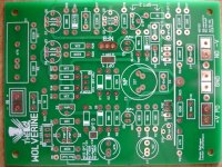
Unfortunately not fit, as the not painted lenght is 0.425", and You have to add the diameters of the terminals (0.025"). I used many of RN60D and RN55D. My experience that 0.4" necessary for RN55D and 0.5" for the RN60D.
Check the attached picture, one of my amplifier board using this values.
Sajti
Attachments
Last edited:
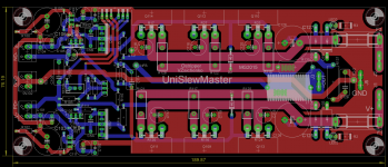
Hi OS and all,
As Borys on his thread explain his finding on using dual layer and closing Gnd Track to Power tracks
I try to apply this to my board layout (picture under). GND is a kind of "partial ground plane". He follow rigth power tracks. Did any one see a issue to do this way?
As Borys on his thread explain his finding on using dual layer and closing Gnd Track to Power tracks
Dual layer pcb gives a lot of advantages. I have made some measurements to compare the standard single layer OPS and dual layer OPS and there is slight measurable improvement in dual layer OPS. I run the V+ and V- rails very close (on top of each other), even better would be to run V+ and V- rails next to each other and putt GND track right above them, if the GND track would be a current return tor speaker than all the electromagnetic should cancel out.
I try to apply this to my board layout (picture under). GND is a kind of "partial ground plane". He follow rigth power tracks. Did any one see a issue to do this way?
Attachments
Krisfr,
That IBM keyboard looks like my logitech is an exact clone of that keyboard. Perhaps they were made by the same manufacturer, I have had mine forever, it has the best key feel of any keyboards I have tried and that was what made me choose it in the first place. Never has given me any problems and every key works as new years later. Still can't believe so many are stuck with using a moose over a trackball. How many of you now have carpal tunnel syndrome, not a nice thing.
By the way I use to make and designed a two piece adjustable keyboard platform with the best ergonomic wrist support I have seen to this day. I sold them to another company that was in that industry and we made thousands of them. you could adjust the height and angle of the wrist support and they were soft self skinning foam construction. I have a couple laying around, they last forever. I sold them the tooling and they tried later to have someone else make the parts, they were never successful, go figure.
Hi OS and all,
As Borys on his thread explain his finding on using dual layer and closing Gnd Track to Power tracks
I try to apply this to my board layout (picture under). GND is a kind of "partial ground plane". He follow rigth power tracks. Did any one see a issue to do this way?
That is good , seen on the "silicon image blameless" kit.
The trend i'm seeing is the tight grouping of 3 or more pairs on the PCB.
2 pair you can get away with it , heat will dissipate symetrically in each
direction . 2-pair will act as 1 BIG pair.
3-pair is different , the center pair will reach SOA much quicker by
the thermal derating. If the OPS is pushed to the limit , this pair will
fail first ..... a weak link in the chain. It will also be "hogging" current ,
pushing it still faster to the ends of SOA.
The electrical and thermal differences between my spaced 3 pair
and tightly packed 5 pair setups are striking. 😱
PS - this effect is greatly reduced with 6-7U heatsinks , heat transmits
in 4 directions - but it still happens here.
OS
Thanks for answer.
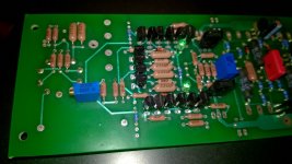
I know the fact about thermal. I try to spread ops as much as i can with available space. But i don't be anxious about that.....as the Vrail will be +/-50VDC. I planed to build a MJL3281/1302 (i have good matched triplets). The package on the picture is the TO264 one so i have a little bit space, they are not so close as in the monster version. For the BJT OPS i have quite generous heatsink (265x140x75mm with 16mm base). The other version i will build is the Vfet one with TO247 margin space will be more consequent. This version will be mount on 300x120x40mm with 10mm base). In both case i think thermal will not be an issue.
The picture under show the 3 situations : TO264/MT200/TO247
Marc
Attachments

Last edited:
Ground planes and such .....
In the "silicon chip" amp kit - Silicon Chip Online - Ultra-LD Mk.2 200W Power Amplifier Module
They do the rail/ground plane "trick" in dual layer. But look at the rest of
their circuit , it straddles these high current inputs(tracks).
I see why they would almost NEED to do this , with this type layout.
Any radiated track fields would infect the low level circuitry they have
almost on top of it.
Our type amps keep the inductor/high currents feeds and returns at
distance. Likely facing the toroid in a typical setup .
Separated by distance and sitting behind 20K virtual capacitance is
the IPS , with it's separate isolated rail feeds and ground.
The OPS's radiated field would only be seen by the very low Z tracks
of the final stage of the EF3 , even the predrivers and Vbe of the Slews
is in a clean zone , separated by distance.
The reason for the twisted/weaved rail lines in power amps , is so they
won't radiate to a low level circuit in passing. Dual layer rails to reduce
L/R would be a better use of the second layer.
A small amp with all on one board might benefit from a layout like the
silicon chip LD (link ). The use of this "trick" is very design dependent.
OS
Last edited:
- Home
- Amplifiers
- Solid State
- Slewmaster - CFA vs. VFA "Rumble"