Also, as the system heats up, the epoxy will expand about twice as fast as the copper. Given that it will be hotter than the copper by design as well, the internal compression will raise forces normal to the chip.
If there is no physical buffer between the chip surface and the epoxy, this will add normal forces to the fray.
Oh, joy. So you may have a setup that works well at room temperature, but cracks the IC beyond some temperature.
Normal forces on transistors can change their characteristics as well as cause them to fail.
Yep. That's rather well-known in the precision DC world. In addition to the temperature stress effects, package stress is another common source of weird offsets and such. In plastic packages, the individual granules of plastic can exert quite a bit of stress on, say, the input pair of an opamp, causing Vos to shift rather dramatically. Stress relief coatings are commonly used to minimize the impact of the package stress on the circuit performance. The package stress can be further minimized by using the TO-99 can or ceramic DIP packages. Sadly, the customers often aren't willing to pay for those.
~Tom
....
You are making the assumption that the tab is filled with solid copper. This is not the case, as I clearly shown in my cross-sections. You can have an LM3886TF X-rayed if you want to make sure, but I would not count on any meaningful thermal conduction through the tab.
...
~Tom
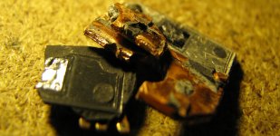
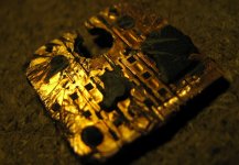
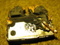
2,2mm holes on tab , same on bottom . tab is filled with solid cooper - two holes like on bottom, and there is some holes beneth die which are filled with this black thing you call epoxy. and wires that go to die are 1.5mm far from front of package
edit: second picture , is that die insulator or die itself?
Attachments
I really appreciate you sharing your notes. Thank you.
You are making the assumption that the tab is filled with solid copper. This is not the case, as I clearly shown in my cross-sections. You can have an LM3886TF X-rayed if you want to make sure, but I would not count on any meaningful thermal conduction through the tab.
I think your calculation of the heat transfer through the sides of the package is assuming that the side of the package is isothermal, no?
I've never seen a plastic package from National/TI that did not have some amount of mold flash. Also, the packages tend to have slanted edges, presumably for mold release. You will have to sand or mill down the packages to make them flat so you can have good heat transfer.
Using your values for the thermal resistance through the top of the package and the back of the package, I arrive at Rth = Rth0 || Rth2 = (2*9)/(2+9) = 1.64 K/W.
I'm taking your area calculations at face value. The calculations do assume that the copper is solid without divots, voids, etc. which from my pictures appears to be a bit of a stretch.
As jneutron points out, sometimes, the IC die is encapsulated in some sort of goop to prevent delamination between the IC and the package material. Furthermore, the top side of the IC is normally covered by an insulator (spin-on glass or similar) of a somewhat uncontrolled thickness to prevent moisture from getting into the IC. The bottom of the IC would be the starting material (probably a doped silicon substrate). This means the thermal path through the bottom of the IC will conduct heat better than that through the top of the die. This means the area of the die should be subtracted from the copper area used for calculating Rth2, or at least, the increase in thermal resistance from the copper slug to the top of the package should be factored into the calculation of Rth2.
I have one burning question, though: WHY? I understand that sometimes it's fun to geek out and completely over-engineer something, but why would I machine blocks of copper to tight tolerances to achieve 1.64 K/W, when an LM3886T with a layer of Bergquist SilPad 1500ST (available from Mouser, et al) would have a thermal resistance around 1.1 K/W?
To get to the 1.64 K/W, you will need a tight (press) fit around the LM3886. Unless you plan to machine each copper block to fit each individual LM3886, you will either not get a good thermal contact or crack the IC package when you tighten the bolts. Neither is desirable.
~Tom
You made a couple of interesting comments, which I would like to take up now.
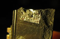
Re. the amount of copper in the tab: your cuts do not tell the whole story. As the photo of tonitonitoni (post #278) shows, in addition to the mounting hole there are four openings in the copper plate through which the upper and lower part of the package are joined (my guess). So I do count on a meanigful heat transfer through the tab - somewhat less than I calculated, but by far not negligible. And I do believe that the designers at National's were rational people who would not have sacrificed this heat transfer area on both sides of the package, as your comment implies.
I mentioned slanted edges in my note and explained how and why I included them in the energy balance. You measured a distance of 1 mm between the copper edge and the side surface, and I increased it by a factor of 2.5 to take into account the slant and the fact that there is only 1.5 mm of copper in the 4.5 mm of package thickness. We can discuss my choice of this parameter but I see no rational reason to ignore this surface in the energy balance.
As regards the upper part of the package I do not see much reason to significantly change the parameter values either. We agreed that the copper plate is isothermal, I think that the epoxy thickness I used is correct, and we could discuss possible reduction of the heat flux from the upper face of the IC to the package face - I wonder by how much you would reduce the heat flow over the IC proper.
As to the WHY question, this was not my subject. I entered the discussion out of curiosity to see whether the claims of better cooling by the copper fixture are technically sound, and because of too much flat denial. Now from the "We all agree about the upper part being useless" we have advanced to discussing the smaller points of the heat transfer through this surface. Not bad, for everyone involved.
Regards,
Braca
2,2mm holes on tab , same on bottom . tab is filled with solid cooper - two holes like on bottom, and there is some holes beneth die which are filled with this black thing you call epoxy. and wires that go to die are 1.5mm far from front of package
edit: second picture , is that die insulator or die itself?
Thank you for the photos tonitonitoni. I missed your post while I was writing.
Regards,
Braca
2,2mm holes on tab , same on bottom . tab is filled with solid cooper - two holes like on bottom, and there is some holes beneth die which are filled with this black thing you call epoxy. and wires that go to die are 1.5mm far from front of package
Plus the hole and slot in the middle of the tab, right. The hole looks to be about 5 mm in diameter.
edit: second picture , is that die insulator or die itself?
It looks like some sort of coating, but it's really tough to tell from the picture. It looks shiny, unlike the rest of the mold compound.
~Tom
Plus the hole and slot in the middle of the tab, right. The hole looks to be about 5 mm in diameter.
It looks like some sort of coating, but it's really tough to tell from the picture. It looks shiny, unlike the rest of the mold compound.
~Tom
According to the DS the mounting hole is 3.8mm dia. I measured the same on my chips.
Regards
I mentioned slanted edges in my note and explained how and why I included them in the energy balance. You measured a distance of 1 mm between the copper edge and the side surface, and I increased it by a factor of 2.5 to take into account the slant and the fact that there is only 1.5 mm of copper in the 4.5 mm of package thickness. We can discuss my choice of this parameter but I see no rational reason to ignore this surface in the energy balance.
We agree that the copper is isothermal. I hope we also agree that the mold compound (black plastic of the package) is NOT isothermal. I could be wrong, but it seems your calculation of A3 leading to Eqn. 12 in your math document assumes that the entire side of the package is isothermal.
I do agree that if you are able to make good thermal contact to the sides of the package, then you need to include those sides in your thermal math - as you did. However, I think A3 should only be the cross-sectional area of the copper, not that of the entire side of the package. This may/may not be what you did in your document. My question is how A3 was derived.
What's the thermal resistance of your thermal goop and how big of a gap have you included to account for the thermal expansion of the IC in your setup?
~Tom
You're right, I assume that the entire lateral surface is isothermal. The error commited is not large since 80% of the area (2x17x3.3mm) is situated where the copper is, and the rest is above of it. In the upper part we have 2D heat conduction, the major part of which is in the vertical direction. By penalizing the larger part of the area by a factor of 2.5 (epoxy thickness 2.5mm instead of 1mm), I think to be on the safe side of the fact that the rest 20% of the area has a lower mean temperature. It is a matter of judgement, since a full 2D analysis is beyond the scope of the calculation.
The colleague who did the experiment tells me that the cold gap was 0.1mm, and that he used elastic heat conducting pads on the flat parts of the package to get the thermal contact. The sides have a larger gap filled with silicon compound.
Regards,
Braca
Last edited:
My instinct is that you want to avoid thermal cycling from creating structural problems on the chip. So it seems like if the device is going to have large swings in demperature, it is necessary to use thermal pads of some sort which will allow better contact at increasing temperatures and loose contact at low temperatures. Perhaps this will also reduce the temperature fluctuation in continueus music playing.
Many years ago, I red an article in some old tech magazine that copper heatsinks reduced
amp distortion due to less internal eddy current build up....
amp distortion due to less internal eddy current build up....
My instinct is that you want to avoid thermal cycling from creating structural problems on the chip. So it seems like if the device is going to have large swings in demperature, it is necessary to use thermal pads of some sort which will allow better contact at increasing temperatures and loose contact at low temperatures. Perhaps this will also reduce the temperature fluctuation in continueus music playing.
No, completely bonkers. If you believe that keeping the die within a narrow temperature range is good, you control either the heat of the heatsink or the dissipation.
Generally its rate of change of temperature that causes the issues (like dunking into iced water). Luckily the people who make these chips have 40 years experience in making ICs reliable . LM3886 has built in protection for high temps so if you just follow the guidelines of the spec it will keep going for years. Given the number of LMs out there over last 15 years they only go bang when in circuits designed by idiots who did not read the specs.
Gents, some notes on the package features.
The epoxy (thermoset) to metal interface bond strength is not a good one. Copper has a TCE (thermal coefficient of expansion) of 16.6 ppm per degree C. Below the glass transition temperature, plastics range from 90 ppm/C for unfilled varieties down to about 35 ppm/C. As a result, there will be large shear stresses between metals and epoxies, especially if the differential TCE is large. For pretty much all epoxies and thermosets, if one goes over the glass transition temperature, there will be a secondary TCE, this time much larger. Also, above the glass transition temp, the plastic becomes soft and loses much of it's lower temperature strength. I use this fact with superconducting magnets by selecting a hardener which provides a glass transition temp in the 45 C range. Rework becomes very easy for the techs as the temp required to soften the epoxy is not too hot to the touch, allowing the use of bare hands where delicate insulations are involved.
The copper leadframe for the parts being examined have a few features which are there to bolster the package integrity. Through holes are there to allow the plastic access to both sides so that the plastic is not relying on it's adhesion to the copper. On the edges, there will sometimes be an angular profile so that the plastic locks into the tab... For large assemblies, we would typically undercut the aluminum case so that the epoxy cannot slip out. At times, we also thread screws into the baseplate for the epoxy to wrap around, again preventing slip.
Cutting the package through on lines sometimes goes through one or more of these features, so without the overall leadframe geometry known, can lead to incorrect conclusions.
Historically, such undercuts were also used to help reduce flux intrusion, but I cannot state if this is currently done.
An interesting thought. It is not correct however, as the eddies in copper are far larger than aluminum. I would be more inclined to think that there was an effect caused by increased eddies, but that it was misinterpreted or not clearly spelled out.
jn
The epoxy (thermoset) to metal interface bond strength is not a good one. Copper has a TCE (thermal coefficient of expansion) of 16.6 ppm per degree C. Below the glass transition temperature, plastics range from 90 ppm/C for unfilled varieties down to about 35 ppm/C. As a result, there will be large shear stresses between metals and epoxies, especially if the differential TCE is large. For pretty much all epoxies and thermosets, if one goes over the glass transition temperature, there will be a secondary TCE, this time much larger. Also, above the glass transition temp, the plastic becomes soft and loses much of it's lower temperature strength. I use this fact with superconducting magnets by selecting a hardener which provides a glass transition temp in the 45 C range. Rework becomes very easy for the techs as the temp required to soften the epoxy is not too hot to the touch, allowing the use of bare hands where delicate insulations are involved.
The copper leadframe for the parts being examined have a few features which are there to bolster the package integrity. Through holes are there to allow the plastic access to both sides so that the plastic is not relying on it's adhesion to the copper. On the edges, there will sometimes be an angular profile so that the plastic locks into the tab... For large assemblies, we would typically undercut the aluminum case so that the epoxy cannot slip out. At times, we also thread screws into the baseplate for the epoxy to wrap around, again preventing slip.
Cutting the package through on lines sometimes goes through one or more of these features, so without the overall leadframe geometry known, can lead to incorrect conclusions.
Historically, such undercuts were also used to help reduce flux intrusion, but I cannot state if this is currently done.
Many years ago, I red an article in some old tech magazine that copper heatsinks reduced amp distortion due to less internal eddy current build up....
An interesting thought. It is not correct however, as the eddies in copper are far larger than aluminum. I would be more inclined to think that there was an effect caused by increased eddies, but that it was misinterpreted or not clearly spelled out.
jn
there was thread where they applyed pressure on front of chip and supposedly they achieved better sound , maybe it has something to do with this clamping method
of topic.
i blew 5-6 3886-s ,1 tf when trying to see how much power they can output with sine at 50hz and huge heatsink,at 42v+- 225va powering single chip and not dummy load but speaker 4r. rest with trying to power small tesla coil with 3886 and flyback from tv. if you consider idiots everyone who try something else than schematics provided in datasheet then why you come on this forums.
i like to test this little chips in ways not intended to work ,needs more thinking and learning why it doesnt work than copy some others working schematics. sry if i misunderstood you english not my native.
of topic.
...... they only go bang when in circuits designed by idiots who did not read the specs.....
i blew 5-6 3886-s ,1 tf when trying to see how much power they can output with sine at 50hz and huge heatsink,at 42v+- 225va powering single chip and not dummy load but speaker 4r. rest with trying to power small tesla coil with 3886 and flyback from tv. if you consider idiots everyone who try something else than schematics provided in datasheet then why you come on this forums.
i like to test this little chips in ways not intended to work ,needs more thinking and learning why it doesnt work than copy some others working schematics. sry if i misunderstood you english not my native.
Last edited:
t
i blew 5-6 3886-s ,1 tf when trying to see how much power they can output with sine at 50hz and huge heatsink,at 42v+- 225va powering single chip and not dummy load but speaker 4r. rest with trying to power small tesla coil with 3886 and flyback from tv. if you consider idiots everyone who try something else than schematics provided in datasheet then why you come on this forums.
i like to test this little chips in ways not intended to work ,needs more thinking and learning why it doesnt work than copy some others working schematics. sry if i misunderstood you english not my native.
Given the thermal protection built in to the LM3886 if you caused one to die the chances are it was going unstable. Some people build them without the Zobel and Thiele networks despite the spec sheet clearly indicating they are needed, those people I would call Idiots.
If you are trying to kill something, or clearly operate it outside its limits for anything other than research your motives may be questionable. The reference schematics in a data sheet are there for a reason. Copying them is often a good starting point until you understand fully why it was done that way.
Do you have any numbers on maximum power to share with us? Or were you just destroying the poor things for lolz? I would be interesting to know at what point they gave up the ghost.
@tonitonitoni
That is cool.
LM3886 like other "brothers" TDA7294 and similar are Power Operational Amplifiers so you can do almost anything you can do with ordinary "small" OPs.
With LM3886 you can build even microphone preamplifier which can work much much better then for example LM741, TL071 or similar.
Or RF power amplifier stage with extraordinary linearity for 2200m radio amateur band 🙂
LM3886 is amassing good IC for it's price and performance!
Hey, I resemble that remark!!if you consider idiots everyone who try something else than schematics provided in datasheet then why you come on this forums.
I have blown some as well, and it was because the idiot didn't follow the datasheet. That idiot being me.
So, no worries..
jn
I should clarify. Cases people post of LM3886 being unreliable in service I have seen all have an implementation where someone has cut corners off the data sheet recommendations probably to save a dollar. I have not seen evidence of a well implemented solution having failures. If there is such evidence i would be interested to find out more. MIL-217F has warped me for life even after a decade of avoiding it.
tf-version got me 13v at 4 R speaker at+-42v for 10 seconds ,there was no zobel ,but neither is on other 2year old working amp with same schematic but on +-38v .
t-version i on +-38v measured 21v at 4r speaker terminals but that speaker was in free air so not valid , and was cheap multimeter so thats why measured at 50hz .
blew one lm just to see that white smoke everyone talks about so only one time lolz.
@yu3ma
7294 also nice chip , but there lot not working ones in croatia(even few lm3875 were some different manufacture maybe not original) so i must stick with 3886. and also 3886 as car audio amp for subwoofers is good (modified sine inverter under hood and actual home use amp in trunk , no wire looses with 3*0.75mm 😀)
MIL-217F has warped me for life even after a decade of avoiding it.
Ah, 217....that explains a lot..😀
I see you are no stranger to pain..
I've been divorced...
OOOh..
Twice.
OHHHHHH!.
jn
- Status
- Not open for further replies.
- Home
- Amplifiers
- Chip Amps
- LM3886 Thermal Experiment (with data)