Picture broke down to pieces
I broke down the picture to pieces in paint and counted pixels. According to that method I got a factor of 4.8 to 1.
EDIT: Skipping the percent calculations and using exact pixel numbers the factor is in fact 4.85:1. (126/237) / (26/237).

I broke down the picture to pieces in paint and counted pixels. According to that method I got a factor of 4.8 to 1.
EDIT: Skipping the percent calculations and using exact pixel numbers the factor is in fact 4.85:1. (126/237) / (26/237).
Last edited:
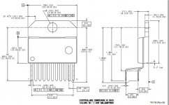
I am only looking at the cross section tom provided, with the ruler next to it.
jn
Well, then you must change your point of view. Go to post #296, it will give you a perfect view of the tab.
Regards
I can clearly see that the copper is a lot thinner than the front covering of packaging plastic.
I would guess at thicknesses that add up to Dni's 3.35mm measurement as 1.86mm for the front plastic, 1.12mm for the copper and 0.37mm for the back plastic.
That gives copper to back as ~3:1 and front to back as ~5:1.
Looking at the cross-sections, that just about tallies with what I can see.
How Dni, could come up with measuring 3.35mm overall thickness and equate to 1.5mm:0.5mm for the plastic thicknesses, I can't fathom. It like using ears as measuring instruments.The epoxy thickness below the copper plate is 0.5 mm (hopefully no objections to that).
Your 5:1 ratio gives 2.5 mm for epoxy thickness above the 1.5 mm thick copper plate.
Summing the above three thicknesses gives overall tab thickness of 4.5 mm.
My 3:1 ratio gives overall tab thickness of 3.5 mm
Tab thickness measured with a digital slide caliper is 3.35 mm.
I would guess at thicknesses that add up to Dni's 3.35mm measurement as 1.86mm for the front plastic, 1.12mm for the copper and 0.37mm for the back plastic.
That gives copper to back as ~3:1 and front to back as ~5:1.
Looking at the cross-sections, that just about tallies with what I can see.
Last edited:
I broke down the picture to pieces in paint and counted pixels. According to that method I got a factor of 4.8 to 1.
View attachment 476618
You analyzed the wrong picture. We've been discussing the mounting tab structure, not the part where the die is situated.
My numbers for the part of the package you analyzed are 1:5.
Regards
I can clearly see that the copper is a lot thinner than the front covering of packaging plastic.
How Dni, could come up with measuring 3.35mm overall thickness and equate to 1.5mm:0.5mm for the plastic thicknesses, I can't fathom. It like using ears as measuring instruments.
I wonder why everybody seems to be overlooking the word tab in my recent posts.
Regards
Maybe because the majority of the heat will pass from the die through the copper to the heatsink by the least resistive route, rather than the more resistive route of going up to the tab to then pass to the heatsink
BTW, I just measured a sample of the T version. 4.40 to 4.45mm thick over the plastic package. I would never dream of buying a thermally crippled TF version.
BTW, I just measured a sample of the T version. 4.40 to 4.45mm thick over the plastic package. I would never dream of buying a thermally crippled TF version.
Maybe because the majority of the heat will pass from the die through the copper to the heatsink by the least resistive route, rather than the more resistive route of going up to the tab to then pass to the heatsink
Andrew, as already mentioned elsewhere, the energy flow follows the path of the least resistance, and at a ratio of the respective thermal conductivities of copper and epoxy of about 400:1, the copper plate will have the same temperature everywhere. Therefore, the conduction of heat towards the heat sink below the die and in the same direction at the tab will be the same. The conduction of heat at the front of the tab towards a heat sink fastened to it will be lower by the ratio of the respective epoxy layer thicknesses, which is 1:3.
Regards
Ah.. The tab.. Missed that 
Anyway, I am looking forward to the future measurements and hopefully we will get some numbers that can prove the total heat transfer capacity of the machined clamp.
Inclined to be a part of the nerd-club I am tempted to solder a 3886T package to a CPU copper heat sink I have in my scrap box and see how low that can get me.
I think we would all be better served by some kind of drawing in support of your thinking. You stated a number under the tab, and another above, which gives a ratio inconsistent with what I call above the tab and below it.Andrew, as already mentioned elsewhere, the energy flow follows the path of the least resistance, and at a ratio of the respective thermal conductivities of copper and epoxy of about 400:1, the copper plate will have the same temperature everywhere. Therefore, the conduction of heat towards the heat sink below the die and in the same direction at the tab will be the same. The conduction of heat at the front of the tab towards a heat sink fastened to it will be lower by the ratio of the respective epoxy layer thicknesses, which is 1:3.
Regards
jn
Last edited:
DNi,
Where did you get the 400 to 1 ratio of copper to epoxy conductivity? Was it from the manufacturer's data you crunched earlier?
I ask because the best epoxy I've used ratio'd to copper as 10 to .06, or about 166.
I suspect the case under consideration has some loading in it to temper it's expansion coefficient, and that would also be to increase it's thermal conductivity.
jn
edit: ALSO...did you do a lateral thermal resistance calculation for the copper?
And, I guess part of the confusion stems from the fact that when I worked in the industry, the entire copper part was called a tab, I believe you are referring to the thinner section where the hole is.
Last edited:
I broke down the picture to pieces in paint and counted pixels. According to that method I got a factor of 4.8 to 1.
EDIT: Skipping the percent calculations and using exact pixel numbers the factor is in fact 4.85:1. (126/237) / (26/237).
View attachment 476618
Armand,
I don't know who's the bigger geek. You, or me.
That was great, thanks for doing that, much appreciated.
john
DNi,
Where did you get the 400 to 1 ratio of copper to epoxy conductivity? Was it from the manufacturer's data you crunched earlier?
I ask because the best epoxy I've used ratio'd to copper as 10 to .06, or about 166.
I suspect the case under consideration has some loading in it to temper it's expansion coefficient, and that would also be to increase it's thermal conductivity.
jn
edit: ALSO...did you do a lateral thermal resistance calculation for the copper?
And, I guess part of the confusion stems from the fact that when I worked in the industry, the entire copper part was called a tab, I believe you are referring to the thinner section where the hole is.
OK, I'm enclosing a sketch with the heat transfer areas defined in the text.
Tab is for me the surface with the red border. And A1+A2 is the heat transfer area at the back of the package, i.e. the contact area at the heat sink.
The lateral surface (blue-bordered) is marked by A3/2 to signify that there are two such surafces at the package.
Now the rest of your points:
The thermal conduction ratio of 400:1 is actually 400:1.3, the figure 1.3 comes from the first calculation in my note; in the reply to Andrew I did not want to go into the fractions. Had I used the thermal resistance of the TF package from the press release of 1995 (1.6K/W) I would have obtained thermal conductance for the epoxy of 2.17 W/(m x K), which would give a ratio in line with your data (185 vs. 166).
I assumed that the lateral thermal conductivity of copper is the same in all three directions - a usual assumption at this level of approximation.
Regards,
Braca
Attachments
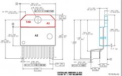
OK, I'm enclosing a sketch with the heat transfer areas defined in the text.
Tab is for me the surface with the red border. And A1+A2 is the heat transfer area at the back of the package, i.e. the contact area at the heat sink.
The lateral surface (blue-bordered) is marked by A3/2 to signify that there are two such surafces at the package.
Now the rest of your points:
The thermal conduction ratio of 400:1 is actually 400:1.3, the figure 1.3 comes from the first calculation in my note; in the reply to Andrew I did not want to go into the fractions. Had I used the thermal resistance of the TF package from the press release of 1995 (1.6K/W) I would have obtained thermal conductance for the epoxy of 2.17 W/(m x K), which would give a ratio in line with your data (185 vs. 166).
I assumed that the lateral thermal conductivity of copper is the same in all three directions - a usual assumption at this level of approximation.
Regards,
Braca
Thanks.
Ok, so you calculated based on manu data, which shifted with time. I'd go with the 185 number. I'm confused however, as you've shown a non isolated package, no? I thought you were talking about the isolated one.
It's ok to assume the copper as isotropic. My question was, did you do a calculation of the thermal drop of the copper laterally. If you assume any heat transfer out near the mounting hole, you have to figure in a lateral thermal density and thermal drop.
jn
Yes, it is a sketch based on the T package (didn't find a TF drawing), but it is only there for information about my partitionig of the heat transfer surfaces. My areas were calculated on the basis of dimensions measured on an isolated LM3886 sample I have.
Yes, I did the lateral heat conduction calculation - it is the area A3 in my note. I assumed isothermal copper plate, and I'm aware of the fact that there are 2D end efects in the lateral direction. This is why I penalized the lateral heat transfer by assuming epoxy thickness of 2.5mm instead of 1mm that Tom measured. The efect of this is reduced lateral heat conduction, and its small influence on the total thermal resistance.
I think my calculation is ample for a first approximation, which is as far as I wanted to go anyway. Going further would have made measured data necessary, which would be the case even if one were to use an FE program to model the assembly in all three directions.
Regards,
Braca
That is a poor model of the heat flow in the copper backplate.Andrew, as already mentioned elsewhere, the energy flow follows the path of the least resistance, and at a ratio of the respective thermal conductivities of copper and epoxy of about 400:1, the copper plate will have the same temperature everywhere. Therefore, the conduction of heat towards the heat sink below the die and in the same direction at the tab will be the same. The conduction of heat at the front of the tab towards a heat sink fastened to it will be lower by the ratio of the respective epoxy layer thicknesses, which is 1:3.
Regards
That is a poor model of the heat flow in the copper backplate.
Assuming that we are discussing here the copper plate within the package, I wonder if you could provide at least an order-of-magnitude analysis to substantiate this claim.
Regards
When the copper plate is dissipating to the heatsink, the isothermal assumption of the copper backplate falls apart.
Ignoring that temperature drop along the backplate leads to significant errors in your model.
That is leading you to seeing conclusions that are not real.
Ignoring that temperature drop along the backplate leads to significant errors in your model.
That is leading you to seeing conclusions that are not real.
Fair enough. Be careful with the tab size however. If the exterior form factor is the same, then they would have stamped the copper smaller for the fully encapsulated version, with holes as well. I do not know how far towards the mounting hole the manu considers as viable heat transfer path, so they may have included more holes for epoxy grab.Yes, it is a sketch based on the T package (didn't find a TF drawing), but it is only there for information about my partitionig of the heat transfer surfaces. My areas were calculated on the basis of dimensions measured on an isolated LM3886 sample I have.
Yes, I did the lateral heat conduction calculation - it is the area A3 in my note. I assumed isothermal copper plate, and I'm aware of the fact that there are 2D end efects in the lateral direction. This is why I penalized the lateral heat transfer by assuming epoxy thickness of 2.5mm instead of 1mm that Tom measured. The efect of this is reduced lateral heat conduction, and its small influence on the total thermal resistance.
I think my calculation is ample for a first approximation, which is as far as I wanted to go anyway. Going further would have made measured data necessary, which would be the case even if one were to use an FE program to model the assembly in all three directions.
Regards,
Braca
As for first approximation, it looks ok. Sometimes we don't have the data we need for a really accurate model.
While you are accurate, it's difficult to model spreading and thermal profile without ansys. Sometimes, simple assumptions are all we have to work with. He's presented to us his model with all it's foibles for discussion. How it tracks good measurement will allow all to determine the accuracy of his model and assumptions.When the copper plate is dissipating to the heatsink, the isothermal assumption of the copper backplate falls apart.
Ignoring that temperature drop along the backplate leads to significant errors in your model. That is leading you to seeing conclusions that are not real.
jn
a.) the copper should be direct to the back of the device using Thermal goop only. This should preferably be by a clamping method rather than the standard offset device hole. 2 holes devices are often better and maybe nearly as good as clamping.
cf. the small cross machined finned sinks. These give a big increase in the FIN surface area but judging by the FIN spacing are intended to benefit from the fans fitted in other parts of the equipment.
The answer is already there. The TF is a complete waste of resources. I can only see justification for the TF in automated assembly plant that must at all costs (including performance) reduce assembly complication.Two question: Since all chips are TF type, If one does not want the copper block to be electrically conductive with the chip, but wants the heat transfer to happen, what is the best interface between the chip and copper: "Pads, non conductive grease, others?????
This seems wrong to me. It might help with a fanned sink where the turbulent flow will pull air through and around the holes. For a non fanned sink, increasing the Thermal Resistance and producing a backplate that is less of an isothermal plate may give nothing extra even though there is a small increase in surface area.Is drilling and countersinking various diameter holes in the aluminum HS block a waste of time, or can it be an aid in the convection process from the HS to the air???.
cf. the small cross machined finned sinks. These give a big increase in the FIN surface area but judging by the FIN spacing are intended to benefit from the fans fitted in other parts of the equipment.
- Status
- Not open for further replies.
- Home
- Amplifiers
- Chip Amps
- LM3886 Thermal Experiment (with data)