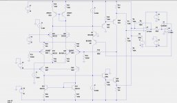
Thanks, I read the Fig 57 and I am trying to simulate. Problem is there is no values for R13 to R19. I guessed and put in 100K for all of them as to voltage at the inputs of the opamp should be close to 0V. I use 1V for V1. I cannot get the simulation going as the output of U2 hung at +13V.Hi Alan0354,
In case you do not already know it, may I suggest you have a look at
figure #57 page #49 of :
http://www.sg-acoustics.ch/analogue_audio/power_amplifiers/pdf/audio_power_amp_design_comments.pdf
Attached is my simulation file so far.
Attachments
Fig 57 appears to be a positive feedback loop to the VAS current. Will not work as is. Try reversing the common mode detector op-amp input.
You'll also need to close the amplifier feedback loop otherwise nothing is there to stop the IPS from saturation due to the extremely high gain. See R10 in the picture.
You'll also need to close the amplifier feedback loop otherwise nothing is there to stop the IPS from saturation due to the extremely high gain. See R10 in the picture.
Attachments
Last edited:
Yes, I figure that much. When I flip the inputs, it sort of working, but when I grounded the collector of Q10 and Q12 and monitor the current of both, the balance goes off when I change the transistor of the IPS.Fig 57 appears to be a positive feedback loop to the VAS current. Will not work as is. Try reversing the common mode detector op-amp input.
I don't want to draw any conclusion at this point, still doing simulation.
One concern also, The way Q13 and Q14 with their emitters connect together, this definitely introduces a lot of noise to the base of Q9 and Q11 as the noise gain from Q13 and Q14 is the impedance at the base of Q9 divided by 2re' of Q13 and Q14 and can be mighty high.
So far, the current of Q10 and Q12 is limited by the setting of V1 so there is no run away current. That is the good news part. BUT when I grounded the collectors of Q10 and Q12. The current of the two transistor change like 40% when I switch one of the 2N2222 of the differential pair to 2N4104.
I am at the process of putting the OPS in and close the GNFB to see whether that help. So far without the OPS, I have to ground the collectors of Q10 and Q12 to avoid any saturation.
Last edited:
Please see my modified .asc in the last post. One of the input transistors Q20 was swapped with a very different yet the VAS current remains rock solid. A large DC offset shows up at the VAS output but that can be dealt with easily with a DC blocking cap in the feedback shunt or with a DC servo.
Please see my modified .asc in the last post. One of the input transistors Q20 was swapped with a very different yet the VAS current remains rock solid. A large DC offset shows up at the VAS output but that can be dealt with easily with a DC blocking cap in the feedback shunt or with a DC servo.
Yes, we cross post a little, I was going to try closing the loop to see, you beat me to it. Yes, it looks pretty good so far. I have to play with it more. But as I pointed out in my last post, I also worry about the noise. I ended up putting a 10K resistor in between the emitters of Q1 and Q2 in the simulation file.
Thanks
I made a play sim of a VAS current stabilizing loop with a opto isolator to sense:
http://www.diyaudio.com/forums/solid-state/56860-optoisolator-vas-bias-comp-diff.html#post637347
http://www.diyaudio.com/forums/solid-state/56860-optoisolator-vas-bias-comp-diff.html#post637347
Thanks, that's interesting. I have been reading your other thread, I just want to verify with you.I made a play sim of a VAS current stabilizing loop with a opto isolator to sense:
http://www.diyaudio.com/forums/solid-state/56860-optoisolator-vas-bias-comp-diff.html#post637347
You use the LED of U1 both as the diode drop for the bias splitter AND more important, to sense the current through the VAS ( of cause through the bias spreader).
The higher the current, the more the transistor in U1 turn on and pull the -ve input of U2 up. If the current through the bias spreader is too high, the output of U2 goes lower and Q13 start to pull current from Q12. Both Q12 and Q13 start pulling current from collectors of Q2 and Q8. This result in increase the current of Q6 and Q4 which reduce the current of Q9 and Q10 ( VAS current). Am I correct?
Also I have a few questions:
1) Can you tell me what is the advantage of using the opto coupler over Fig.57 I simulated?
2) Do you still have the LTspice file as your other post is from 2005!!
3) The way I am implementing my amp is I have the OPS on a separate board, that means the bias spreader is on the other board. Also, I want all the transistor and diode of the bias spreader mounted on the main heat sink. So using the opto coupler inside the bias spreader is out of the question for me. But I should be able to put the diode in series with the output of the VAS.....eg. Between the bias spreader and Q10 in your schematic. Do you see any problem with this? That way, the opto coupler will be on the IPS VAS board.
4) A side question, I notice you use 3EF with NPN top and PNP bottom. I am planning to use 3EF, but I am still debating whether I want to use one PNP EF on top and one NPN EF at the bottom to decrease the voltage needed on the bias spreader. I wonder what's your opinion.
5) Did you build the circuit? How does it sound?
Thanks
Last edited:
from before diyAudio allowed .asc attachments - save the .txt attachment and change the extension to .asc and it should work in LTspice
just an armchair exercise to me - I don't build power amps - just headphone amp sized circuits
but I do like doing EE "puzzles" and discrete design offers more scope to keep the mind exerised
just an armchair exercise to me - I don't build power amps - just headphone amp sized circuits
but I do like doing EE "puzzles" and discrete design offers more scope to keep the mind exerised
I went through all the thermal and electrical simulations for my "similar" IPS .
I have not noticed any real variation of VAS current from the open door (-5C) to my
hot work area. Maybe , the Hawksford is cancelling thermally (as simulated).
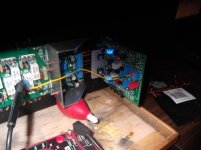
Still , I had to actually build it (below)
... and change some values to get < .1ma stability.
I used the "nearly useless" DMM Hfe test 😛 . This made for <50mv offset before
I plugged in the servo.
I simulated the actual fig. 57 example and built a beta enhanced VAS , it was
much harder to stabilize ( and still can't beat the Hawksford VAS - thd wise)
I "played" with 3 different versions ranging from the fig. 57 to the simplest 6 device
version for IPS/VAS - none negotiate 30-75V rails and -5C - + 40C like (below 2).
PS - fig 57 is "concept" - real is a much more time consuming endeavor.
OS
I have not noticed any real variation of VAS current from the open door (-5C) to my
hot work area. Maybe , the Hawksford is cancelling thermally (as simulated).
Still , I had to actually build it (below)
... and change some values to get < .1ma stability.
I used the "nearly useless" DMM Hfe test 😛 . This made for <50mv offset before
I plugged in the servo.
I simulated the actual fig. 57 example and built a beta enhanced VAS , it was
much harder to stabilize ( and still can't beat the Hawksford VAS - thd wise)
I "played" with 3 different versions ranging from the fig. 57 to the simplest 6 device
version for IPS/VAS - none negotiate 30-75V rails and -5C - + 40C like (below 2).
PS - fig 57 is "concept" - real is a much more time consuming endeavor.
OS
Attachments
You guys are drowning me. I am working harder than when I was working in the last few days.......say weeks!!!! Something is wrong with this picture!!!😛😀😱
I still thinking about using matched differential pair transistors. That seems to be the key. With that, I might be able to use the simplest circuit in Fig. 7.10 in Mr. Cordell's book. I can even consider using matched JFET pairs.
I still thinking about using matched differential pair transistors. That seems to be the key. With that, I might be able to use the simplest circuit in Fig. 7.10 in Mr. Cordell's book. I can even consider using matched JFET pairs.
Last edited:
Have you read the chapter "Midnight Programming" in Tracy Kidder's book, "Soul of a New Machine"?You guys are drowning me. I am working harder than when I was working in the last few days.......say weeks!!!! Something is wrong with this picture!!!😛😀😱
(More info at: 16F616 ADC Questions | Microchip )
Dale
Hi Alan,
I've revisited the circuit of Figure 7.10, and I now do not believe that circuit is reliable with the values of 47k in the differential shunts across the current mirrors. I re-did sensitivity simulations by placing offset voltage sources in series with various bases. Although I do not believe that beta mis-match is the big problem, Vbe matching is a big enough problem to make that circuit, with 47k, not recommendable.
It looks like any one offset of 1mV in any of the differential or current mirror pairs can cause as much as 10% change in VAS standing current. And there are 4 transistor pairs where this can happen, resulting in a significant spread of VAS idle current, especially when the worst-case combination of offsets occurs. The problem simply is that the 47k load allows too much gain for the offsets to be amplified by.
How about using matched pairs from Q1 & Q2, Q3 and Q4 in Fig. 7.10? Something like a MAT01 etc.?
Q5 & Q6, Q7 and Q8 do not seem to be nearly as critical because of Q13 and Q14 buffering. Maybe I can get away with not matching, OR buy a cheaper dual transistor instead of expensive matched pairs.
The key is thermal tracking, the Vbe difference inside the IC is very small.
What do you think?
Also, seems like I can put trim pot for R6 and R8 can adjust the top and bottom current of the VAS individually. We are talking about really high end amps, hand pick, matching pairs and custom trim is not exactly that bad. Not to mention I am not planning to sell as product, just build one for myself. As long as the long term stability is good enough, it's good enough!!! I really don't want to get into DC servo if I can help it. Not because of complication, but because like in your chapter, the servo can get in the way of the low frequency response and introduce distortion.
Last edited:
Ha ha!!! No!!! I am drowning in reading posts here, reading books and articles. I am up till 3AM every night!!!! I just decided to go SS instead of tubes around Christmas and I have been cramping since. I never worked on SS audio until now. The only audio amp I worked on were tube guitar amps....which, have very little in common with this.Have you read the chapter "Midnight Programming" in Tracy Kidder's book, "Soul of a New Machine"?
(More info at: 16F616 ADC Questions | Microchip )
Dale
Yes, I am having the time of my life, but it's exhausting.
?
Not because of complication, but because like in your chapter, the servo can get in the way of the low frequency response and introduce distortion.
Total balony ... in fact , it is the typical DC blocking cap that has the highest <50hz THD.
Some of the best dedicated AB sub amp plates are comp.diff. with servo.
PS - it "CAN" ... it does not have to. Many a "audiophile" 3000$ amp
will use a servo. In fact , most do.
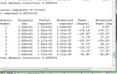
Boy ! , that's a lot of thd (below) at 20hz. 🙄 😛
I don't have the AP analyzer to see the .83ppm , but the offset actually is
.3mv on the real thing.
"Next gen servo's" bias the CCS's and don't even touch the sacred audio path.
Have one of them also perfected. 😀
OS
Attachments
OStripper, can you send me a link to your comp diff design that with tail current source servos? Cheers.
That's what's in the book.Total balony ... in fact , it is the typical DC blocking cap that has the highest <50hz THD.
Some of the best dedicated AB sub amp plates are comp.diff. with servo.
PS - it "CAN" ... it does not have to. Many a "audiophile" 3000$ amp
will use a servo. In fact , most do.
Boy ! , that's a lot of thd (below) at 20hz. 🙄 😛
I don't have the AP analyzer to see the .83ppm , but the offset actually is
.3mv on the real thing.
"Next gen servo's" bias the CCS's and don't even touch the sacred audio path.
Have one of them also perfected. 😀
OS
Can you show the complete schematic of your servo? The one you posted is not complete, I didn't see where the input of the opamp from.
OStripper, can you send me a link to your comp diff design that with tail current source servos? Cheers.
They are CFA's , I'm working on another leach with this now (now).
OS
Alan0354,
You sparked up some enlightening conversation = good stuff 🙂
Why not use one of "ostripper" complementary IPS? Seems to be designs that has/have been sim'd and tested with good results and correlation.
Oh, they are all CFA!! types
I was looking at building fig 7.13, I have it sim'd but yet to fab/test anything. if I do I will layout use either BF862 or LSK389/489 types and a servo too!! I will attach the sim for it.
Anyone care to comment about fig 7.13 design?
Attachments
Last edited:
That's what's in the book.
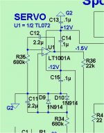
Can you show the complete schematic of your servo? The one you posted is not complete, I didn't see where the input of the opamp from.
(below)- standard 2500$ HK990 servo. R34 comes from the output stage
R36 is the same value as the main feedback resistor and goes to the
LTP inverting input. Fc of about .2hz.
Uses common TL072 IC.
Seen many old similar circuits in 20-30 year old Japanese amps using
ne5332 - one half for each channel. NONE were defective.
These old circuits with the old 5532 do not settle as quick as the
one below or go to .1-.3mv as readily. 🙁 But they work for
decades !
Don't be scared of servo's !
I also have ran my amps without the servo - no audible difference.
OS
Attachments
How about using matched pairs from Q1 & Q2, Q3 and Q4 in Fig. 7.10? Something like a MAT01 etc.?
Q5 & Q6, Q7 and Q8 do not seem to be nearly as critical because of Q13 and Q14 buffering. Maybe I can get away with not matching, OR buy a cheaper dual transistor instead of expensive matched pairs.
The key is thermal tracking, the Vbe difference inside the IC is very small.
What do you think?
Also, seems like I can put trim pot for R6 and R8 can adjust the top and bottom current of the VAS individually. We are talking about really high end amps, hand pick, matching pairs and custom trim is not exactly that bad. Not to mention I am not planning to sell as product, just build one for myself. As long as the long term stability is good enough, it's good enough!!! I really don't want to get into DC servo if I can help it. Not because of complication, but because like in your chapter, the servo can get in the way of the low frequency response and introduce distortion.
Hi Alan,
Matched pairs will help. I always use dual monolithic matched pairs in my IPS LTP, but not p-type devices because I usually just use a unipolar IPS. So I just use NPN pairs or N-channel JFET pairs.
I don't recall saying those things about a DC servo, at least not for a properly designed one. DC servos are generally superior. As with any part of an audiophile amplifier, they should be designed with attention to detail. I use them all the time.
Cheers,
Bob
- Home
- Amplifiers
- Solid State
- Bob Cordell's Power amplifier book