You mean the figure of 8 trick, right?
Cheers, E.
This trick makes sense. Thank you to Andrew and Edmond for pointing it out. Trying it out for the SuperTis front end. Aesthetically, it appears to work but now trying to get my head round the currents in the loops and whether the magnetic fields will cancel out (or not).
Paul
Hi Mr. Cordell
This is Alan
I did try that at the beginning. Attached is the original file before I simplified to one sided. The result seems to be worst. For one, I originally use 2mA tail current. Lowering the tail current improve the situation, but if I follow the 10:1 degeneration, The gain is going to get low and won't be much better than just using resistor load.
Thanks.
Hi Alan,
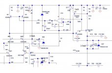
I've revisited the circuit of Figure 7.10, and I now do not believe that circuit is reliable with the values of 47k in the differential shunts across the current mirrors. I re-did sensitivity simulations by placing offset voltage sources in series with various bases. Although I do not believe that beta mis-match is the big problem, Vbe matching is a big enough problem to make that circuit, with 47k, not recommendable.
It looks like any one offset of 1mV in any of the differential or current mirror pairs can cause as much as 10% change in VAS standing current. And there are 4 transistor pairs where this can happen, resulting in a significant spread of VAS idle current, especially when the worst-case combination of offsets occurs. The problem simply is that the 47k load allows too much gain for the offsets to be amplified by.
Reducing the 47k resistors by a factor of about 10 to perhaps 4.7k should make the circuit adequately reliable with reasonably matched transistors, but with correspondingly much less DC open-loop gain for the amplifier. This will reduce the open-loop gain to the vicinity of that achieved with the ordinary resistive load instead of a current mirror. Although huge amounts of open loop gain at low frequencies is not the be-all and end-all of amplifier design, this does bring into question how much value this circuit brings to the table.
I have not looked into it, but the current mirror circuit with the smaller value of differential shunt resistance may still help keep the differential pairs in balance as compared to the simple resistive load approach.
It is notable that the simple resistor approach will also have tolerance problems in setting the VAS standing current for all of the same reasons. It is tempting to speculate that if the DC gain of the input stage to the VAS input node is the same, then the sensitivity to differential pair mismatch may be about the same for the simple resistor approach and the shunted current mirror approach.
All of this gives more pause in regard to using the full complementary input stage that has been used by so many in the past - without a more sophisticated approach like Edmond's.
Finally, with regard to IPS gain, which is at issue here, we do need to be mindful that too low an amount of IPS gain will invite increased input-referred noise from the VAS circuitry. Where possible, it is nice to have IPS gain of 10 or more to swamp out VAS noise.
Most of these issues go away when we use a unipolar input stage, foregoing the full complementary architecture. I have always been more comfortable with the unipolar IPS, but it is certainly not as pretty to look at.
Cheers,
Bob
Hi Alan,
It looks like any one offset of 1mV in any of the differential or current mirror pairs can cause as much as 10% change in VAS standing current. And there are 4 transistor pairs where this can happen, resulting in a significant spread of VAS idle current, especially when the worst-case combination of offsets occurs. The problem simply is that the 47k load allows too much gain for the offsets to be amplified by.
Reducing the 47k resistors by a factor of about 10 to perhaps 4.7k should make the circuit adequately reliable with reasonably matched transistors, but with correspondingly much less DC open-loop gain for the amplifier. This will reduce the open-loop gain to the vicinity of that achieved with the ordinary resistive load instead of a current mirror. Although huge amounts of open loop gain at low frequencies is not the be-all and end-all of amplifier design, this does bring into question how much value this circuit brings to the table.
I have not looked into it, but the current mirror circuit with the smaller value of differential shunt resistance may still help keep the differential pairs in balance as compared to the simple resistive load approach.
Most of these issues go away when we use a unipolar input stage, foregoing the full complementary architecture. I have always been more comfortable with the unipolar IPS, but it is certainly not as pretty to look at.
Cheers,
Bob
Hi Mr. Cordell
Thanks for taking the time. I am disappointed, BUT I am not totally given up on this. I am actually looking into expensive matched transistor pairs like MAT01 and MAT02 and others for the input differential pairs. From my simulation, the current mirror is not nearly as sensitive to mismatch.
Also, one other thing that I looked into and was really surprising was how much the base current affect the bias current of the VAS. A slight difference in beta between the diferential pair can create a few mV of offset and cause the imbalance current to flow through R14. I simulated to verify the imbalance ended up going through the R14 to cause all the problems. I am actually consider using match JFET pairs to do away with all the input current.
Now, I am also looking into single differential pair IPS instead of complementary. Many of the designs do that. BUT there is a potential problem in using single ended LTP as IPS. There is a lot of ways to implement symmetrical VAS.........But I have question about implementing miller cap in symmetrical VAS.I am looking at Fig.7.15 of page 145. C1 is the miller cap. But notice this only on one side of the two output from the IPS. So it is not like you have symmetrical miller caps on both sides. Also the miller effect is on the top side of the bias spreader, so the other side(collector of Q14) really does not have the true pole splitting as there is a the bias spreader in between. Can I count on the impedance across the bias spreader is low enough that it's like an AC short circuit? If miller cap on only one side like this works, then there is hope!!!
I read your book on how miller cap lower the output impedance of the VAS as higher frequency, this will lessen the effect of the input impedance change of the OPS at large signal. Do you think 3EF can give high enough input impedance to avoid loading the VAS?
I am re-reading your book over and see what I missed the first time. Also I want to read the Spice simulation also.
Engineering is an art of compromising, so far, there is no perfect solution!!! Question is what to give up.
Thanks
Last edited:
Hi Mr. Cordell
Thanks for taking the time. I am disappointed, BUT I am not totally given up on this. I am actually looking into expensive matched transistor pairs like MAT01 and MAT02 and others for the input differential pairs. From my simulation, the current mirror is not nearly as sensitive to mismatch.
Also, one other thing that I looked into and was really surprising was how much the base current affect the bias current of the VAS. A slight difference in beta between the diferential pair can create a few mV of offset and cause the imbalance current to flow through R14. I simulated to verify the imbalance ended up going through the R14 to cause all the problems. I am actually consider using match JFET pairs to do away with all the input current.
Now, I am also looking into single differential pair IPS instead of complementary. Many of the designs do that. BUT there is a potential problem in using single ended LTP as IPS. There is a lot of ways to implement symmetrical VAS.........But I have question about implementing miller cap in symmetrical VAS.I am looking at Fig.7.15 of page 145. C1 is the miller cap. But notice this only on one side of the two output from the IPS. So it is not like you have symmetrical miller caps on both sides. Also the miller effect is on the top side of the bias spreader, so the other side(collector of Q14) really does not have the true pole splitting as there is a the bias spreader in between. Can I count on the impedance across the bias spreader is low enough that it's like an AC short circuit? If miller cap on only one side like this works, then there is hope!!!
I read your book on how miller cap lower the output impedance of the VAS as higher frequency, this will lessen the effect of the input impedance change of the OPS at large signal. Do you think 3EF can give high enough input impedance to avoid loading the VAS?
I am re-reading your book over and see what I missed the first time. Also I want to read the Spice simulation also.
Engineering is an art of compromising, so far, there is no perfect solution!!! Question is what to give up.
Thanks
If you would care to use the excellent search engine, and then read the results, on this forum, you would find 99.9% of the answers you are looking for, discussed and analyzed in extenso, from both theoretical and practical perspectives.
Otherwise, I am sure Mr. Cordell has a reasonable hourly rate, in particular when it comes to helping engineers with
30 years of designing RF, analog IC and all different complicated analog electronics
Last edited:
Yeh, I am dumb, can you help finding the answer for me?If you would care to use the excellent search engine, and then read the results, on this forum, you would find 99.9% of the answers you are looking for, discussed and analyzed in extenso, from both theoretical and practical perspectives.
Otherwise, I am sure Mr. Cordell has a reasonable hourly rate, in particular when it comes to helping engineers with
Yeh, I am dumb, can you help finding the answer for me?
No.
If you would care to use the excellent search engine, and then read the results, on this forum, you would find 99.9% of the answers you are looking for, discussed and analyzed in extenso, from both theoretical and practical perspectives.
Otherwise, I am sure Mr. Cordell has a reasonable hourly rate, in particular when it comes to helping engineers with
Waly there is no need for you to be putting other people down.
This comment is truly out of order, especially coming from somebody whose profile describes himself as a "student". The conversation between "Alan0354" and Bob Cordell is a great example of sincere scholarship and quest for understanding, conducted between a student and teacher, mentor and protege, or master and apprentice. It's the kind of conversation Jim Williams (an autodidact) must have had with Bob Pease or Barrie Gilbert. It's the sort of discussion that must have occurred "on the train from Berlin", where the atomic physicists of the 1930's worked out the structure of the atom, as described by Dr Jacob Bronowski in Chap 11 of "The Ascent of Man". It's the kind of conversation that generates advances in science and engineering.If you would care to use the excellent search engine, and then read the results, on this forum, you would find 99.9% of the answers you are looking for, discussed and analyzed in extenso, from both theoretical and practical perspectives.
Otherwise, I am sure Mr. Cordell has a reasonable hourly rate . . .
I know first-hand the satisfaction of sharing something you have mastered with somebody who admires and respects your mastery. I also know first-hand the anger and contempt of encountering people who seek to exploit, abuse, and devalue one's mastery. These two Forum members are experiencing that first type of relationship, not the second.
Dale
Hi Mr. Cordell
I really like the idea of complementary LTP with current mirror and symmetrical VAS. I am thinking along the line of DC servo that put a simple circuit that control the voltage at the emitter of Q10 in Fig.7.10. I should be able to do the same thing at the bottom also. It does not have to be accurate, all it matters is to keep the voltage so the current of the VAS is about 10mA. The GNFB should be able to come in and balance the rest. I am thinking in terms of floating a cheap opamp to the rail to do the job. Something like a TL081 jFET input. No need to get fancy ones.
Then we won't need R14 and truly make the current mirror load high impedance. Might have to eliminate Q13 and connect Q5 as diode. The DC servo feedback then connect to the base of Q5 and Q6. The idea is same as yours in Fig.7.16 where Q7 and Q8 set the voltage at the base of Q6 and Q7 to control the voltage.
Last edited:
Hi Mr. Cordell
It's too late to edit the last post, but this is kind of what I am thinking. I just throw in the opamp, have not really thought out the detail, but that the rough idea and see whether there is any hope.
Basically, I try to force the emitter of Q7 to about 1.9V to set the current of the VAS. Do the same think at the bottom half of the LTP and use GNFB to balance the whole amp.
Thanks
Attachments
Last edited:
Current mirror noise
Hi Bob,
You made a good point, which spurred me to have a closer look at the noise contribution from the current mirrors. If the (Johnson) noise from the feedback resistors and input LP filter were excluded, indeed, noise from the current mirrors do have a profound effect on the overall noise figure. A bit counter intuitive at first sight: the lower RE (of the CM's), the more noise.
But in real life with practical feedback resistors and an input filter, this noise contribution is relative small. If low noise trannies are also used for the current mirrors, it is not too much to worry about.
Cheers, E.
Hi Alan,
[..]
Finally, with regard to IPS gain, which is at issue here, we do need to be mindful that too low an amount of IPS gain will invite increased input-referred noise from the VAS circuitry. Where possible, it is nice to have IPS gain of 10 or more to swamp out VAS noise.
[..]
Cheers,
Bob
Hi Bob,
You made a good point, which spurred me to have a closer look at the noise contribution from the current mirrors. If the (Johnson) noise from the feedback resistors and input LP filter were excluded, indeed, noise from the current mirrors do have a profound effect on the overall noise figure. A bit counter intuitive at first sight: the lower RE (of the CM's), the more noise.
But in real life with practical feedback resistors and an input filter, this noise contribution is relative small. If low noise trannies are also used for the current mirrors, it is not too much to worry about.
Cheers, E.
Common mode control loops are know to real analog (IC) designers since the 70's. Since then, this concept moved to undergrad Analog Design courses, and here's an example. Of course, such undergrad courses require a little more of an abstract understanding effort, certainly more than for digesting half baked schematics. But nothing that engineers with 30 years experience cannot handle.
Keyword for searching this forum: CMCL
315 posts found.
Keyword for searching this forum: CMCL
315 posts found.
Hi Alan0354,
In case you do not already know it, may I suggest you have a look at
figure #57 page #49 of :
http://www.sg-acoustics.ch/analogue_audio/power_amplifiers/pdf/audio_power_amp_design_comments.pdf
In case you do not already know it, may I suggest you have a look at
figure #57 page #49 of :
http://www.sg-acoustics.ch/analogue_audio/power_amplifiers/pdf/audio_power_amp_design_comments.pdf
Most of these issues go away when we use a unipolar input stage, foregoing the full complementary architecture. I have always been more comfortable with the unipolar IPS, but it is certainly not as pretty to look at.
Hi Bob,
"certainly not as pretty to look at"... if we suppose that symmetry is aesthetically superior. I suspect that the main reason why there is so much interest for full complementary architecture relies more in a kind of fascination for symmetry than anything else.
I've revisited the circuit of Figure 7.10, and I now do not believe that circuit is reliable with the values of 47k in the differential shunts across the current mirrors.
Ah what a shame... I produced a circuit and spent a fair bit of time doing the layout for a Figure 7.10 front-end coupled to a nice OPS. The differential were reduced to 22k to reduce sensitivity, but if they need to reduce further to 4k7 or thereabouts then I hardly see the point of pursuing this project for the marginal gains vs. simple resistive collector loads.
But I'm glad to know now rather than spend more time assembling and debugging the circuit.
Time to go back to my simpler enhanced D. Self IPS + S. Groner EF3 OPS, I think, and start to explore H. Dymond's improved Cdom connection.
Edmond's 'Super TIS' seems to be the most promising of the of the advanced fully balanced designs, and I will be keen to give that a try once my PCB skills improve. This would be interesting to do on a 4 layer PCB or perhaps 6 layer PCB with interleaved ground planes?
Hi Bob,
A bit counter intuitive at first sight: the lower RE (of the CM's), the more noise.
Cheers, E.
Not at all, it's obvious that a lower RE will give more noise.
The same with a CCS, the noise depends on the voltage drop on the RE.
The higher RE voltage drop the better, but then you'll have to sacrifice some gain.
I've found that a RE voltage drop around 5V gives the best performance ( noise vs gain). I have the formula if you're interested. 🙂
And as you say low noise trannies in the CM and CCS is important. If it's done right, rb of the CM and CCS trannies will decide the noise.
Stein
Ah what a shame... I produced a circuit and spent a fair bit of time doing the layout for a Figure 7.10 front-end coupled to a nice OPS. The differential were reduced to 22k to reduce sensitivity, but if they need to reduce further to 4k7 or thereabouts then I hardly see the point of pursuing this project for the marginal gains vs. simple resistive collector loads.
If you have the pcb and the parts don't give up just yet. If you have the kind of DVM that measure hfe etc., you might be able to match the transistors before putting them in.
I don't think you even need to solder in the expensive power transistor, just the IPS and VAS. Ground the bias spreader on both side and read the voltage at the emitter of the VAS to determine the current to see how far it is off. This is just like how I simulate in post 5040. If it is within the safe limit, then it's not too bad. I believe once you match the transistor to get the current into the ball park ( in my case between 7.5 to 12.5mA), it's not going to drift off. You can then decide whether you want to move forward or not. You don't have much to loose as you already have the pcb, the IPS and VAS are cheap.
In my case, I am still reading, but I am not ruling out using precision matched pair for the differential pairs. Or even using matched N and P JFET.
JMHO
the hFE function of most dmm is nearly useless.
It measures at a nearly fixed tiny Ib and results in an unknown Vbe and unknown Ic for the stated hFE.
You need Vbe, Ib, Ic and the junction temperature to give a useful set of data to match transistors.
You can with an appropriate measuring jig remove most of the effects of an unknown Tj, but you still NEED the other three.
You need to allow for Tj, because Vbe and hFE are affected by Tj.
Not at all, it's obvious that a lower RE will give more noise.
The same with a CCS, the noise depends on the voltage drop on the RE.
The higher RE voltage drop the better, but then you'll have to sacrifice some gain.
I've found that a RE voltage drop around 5V gives the best performance ( noise vs gain). I have the formula if you're interested. 🙂
And as you say low noise trannies in the CM and CCS is important. If it's done right, rb of the CM and CCS trannies will decide the noise.
Stein
This is exactly right. One way of looking at it is that the voltage noise of the current mirror transistor is forced across its RE, causing a noise current. So smaller RE makes more noise current for a given transistor noise voltage. This also means that the lower the transconductance of the input LTP, the higher the input-referred noise resulting from the current mirror noise. This part of the argument holds even if the RE are ideal noiseless resistors. Current mirrors with little or no degeneration resistance (RE) can be a significant noise source.
Unfortunately, the value of RE that we can use is often limited in practice by considerations relating to the interface to the VAS, due to the DC drop across RE. Indeed, the use of the Darlington VAS can sometimes help in this regard by providing one Vbe more of headroom for the current mirror.
The IPS/VAS I used in my MOSFET power amplifier, with a differential current source load and a differential VAS, breaks this constraint if one is willing to give up some rail voltage headroom or use boosted supplies for the front-end of the amplifier.
Cheers,
Bob
- Home
- Amplifiers
- Solid State
- Bob Cordell's Power amplifier book