That's what's in the book.
Can you show the complete schematic of your servo? The one you posted is not complete, I didn't see where the input of the opamp from.
Alan,
please point me to the actual page in the book to which you are referring. If what I have written is not adequately clear such that it misled you, then it will mislead others and I need to correct it in the next edition.
Cheers,
Bob
Alan0354,
You sparked up some enlightening conversation = good stuff 🙂
Why not use one of "ostripper" complementary IPS? Seems to be designs that has/have been sim'd and tested with good results and correlation.
Oh, they are all CFA!! types
I was looking at building fig 7.13, I have it sim'd but yet to fab/test anything. if I do I will layout use either BF862 or LSK389/489 types and a servo too!! I will attach the sim for it.
Anyone care to comment about fig 7.13 design?
No - 7 are VFA , 3 are CFA.
.Even the forum's amp .. VFA.After they are listening to one of these , I often
recommend Bob's book to learn more - or to "tweak" (refine) what they have built.
OS
Thanks, I read the Fig 57 and I am trying to simulate. Problem is there is no values for R13 to R19. I guessed and put in 100K for all of them as to voltage at the inputs of the opamp should be close to 0V. I use 1V for V1. I cannot get the simulation going as the output of U2 hung at +13V.
Attached is my simulation file so far.
You may ask Samuel Groner who is a DiyAudio member.
Sorry, I must be seeing things. I could swear I saw that the servo might interfere with the very low frequency. My head is spinning as I've been reading different articles, designing.........I need vacation........from my hobby!!!!Alan,
please point me to the actual page in the book to which you are referring. If what I have written is not adequately clear such that it misled you, then it will mislead others and I need to correct it in the next edition.
Cheers,
Bob
I think that has been resolved. The drawing has an error, other than that, it looks like it's working from simulation.You may ask Samuel Groner who is a DiyAudio member.
Thanks
Hi Alan,
Matched pairs will help. I always use dual monolithic matched pairs in my IPS LTP, but not p-type devices because I usually just use a unipolar IPS. So I just use NPN pairs or N-channel JFET pairs.
Cheers,
Bob
You think unipolar IPS is as good as complementary? That will resolve a lot of issue!!! I am looking into match JFET pairs to get away with the problem with input bias current.
Thanks
Thanks, I got that part of the schematic, but where is the input of the opamp comes from?(below)- standard 2500$ HK990 servo. R34 comes from the output stage
R36 is the same value as the main feedback resistor and goes to the
LTP inverting input. Fc of about .2hz.
Uses common TL072 IC.
Seen many old similar circuits in 20-30 year old Japanese amps using
ne5332 - one half for each channel. NONE were defective.
These old circuits with the old 5532 do not settle as quick as the
one below or go to .1-.3mv as readily. 🙁 But they work for
decades !
Don't be scared of servo's !
I also have ran my amps without the servo - no audible difference.
OS
Thanks
You think unipolar IPS is as good as complementary? That will resolve a lot of issue!!! I am looking into match JFET pairs to get away with the problem with input bias current.
Thanks
Yes, I think they are as good or better. I used a unipolar JFET IPS in my MOSFET power amplifier from the early 80s. I like JFET inputs and P-channel dual monolithis JFETs are unobtanium.
Cheers,
Bob
Thanks, that's the magic words!!!! I try so hard only because of you talking about the complementary IPS.Yes, I think they are as good or better. I used a unipolar JFET IPS in my MOSFET power amplifier from the early 80s. I like JFET inputs and P-channel dual monolithis JFETs are unobtanium.
Cheers,
Bob
The other really important question is the symmetrical VAS. I know the symmetrical VAS has advantage on symmetrical slew rate. BUT how about if I increase the bias current of the VAS to say 20mA or above so the slew rate is way beyond the required for the best audiophile?
If I can use 20mA or higher CCS for one side of the VAS, the whole thing becomes very easy!!! I already planned to use two transistor in darlington for VAS, I can easily use medium power transistor for the second transistor and run 20mA+. This on top of I am using 3EF for OPS. That should do it!!!
Please let me know.
Thanks
Last edited:
...
BUT how about if I increase the bias current of the VAS to say 20mA or above so the slew rate is way beyond the required for the best audiophile?
Hi Alan,
Have you considered Miller Input Compensation? Good for achieving fast slew rates.
Paul
Thx, you have too many for me to keep track of, all great examples BTW!!No - 7 are VFA , 3 are CFA
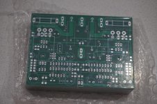
Hi guys
My boards arrived today however I'm not convinced that it is worth pursuing this project given the recent conversation re. Figure 7.10.
If the gain has to be reduced to the point where a simple LTP collector load is able to close in on its performance, I'd probably just build a Leach or jump into Edmond's Super TIS.
Any thoughts?
Cheers
Christian
Attachments

I still think you should at least hand pick transistors and build just the IPS and VAS like I suggested in post 5078. The only thing you need to look for is the max current from both the top and the bottom VAS when you ground the middle. They don't even need to be balance, just make sure they are within 7.5mA to 12.5mA. You are in the ball part. The GNFB will take care for the final balance.Hi guys
My boards arrived today however I'm not convinced that it is worth pursuing this project given the recent conversation re. Figure 7.10.
If the gain has to be reduced to the point where a simple LTP collector load is able to close in on its performance, I'd probably just build a Leach or jump into Edmond's Super TIS.
Any thoughts?
Cheers
Christian
Are you trying to sell the amp? If not, there is nothing wrong with hand pick transistors. OR even adding a trim pot. It would be a waste to dump the stack of boards.
I am on my 4th designs, everyone has good and bad points, none is perfect. I would experiment with the pcb if I were you. What make you think you won't encounter problem with the other designs?
Last edited:
Hi Alan,
Have you considered Miller Input Compensation? Good for achieving fast slew rates.
Paul
I like MIC. I used it in my MOSFET amplifier back in the early 80s. Even though the amplifier was only 50 wpc, it achieved 300V/us. It used a push-pull VAS.
Cheers,
Bob
Hi guys
My boards arrived today however I'm not convinced that it is worth pursuing this project given the recent conversation re. Figure 7.10.
If the gain has to be reduced to the point where a simple LTP collector load is able to close in on its performance, I'd probably just build a Leach or jump into Edmond's Super TIS.
Any thoughts?
Cheers
Christian
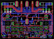
Nice looking board! I'd build it with the 47k resistors reduced to perhaps 4.7k. With this circuit, you are still ahead of the game as compared to a simple resistive IPS load. In referring to the Leach, IIRC, he just uses the full-complementary input stage with simple resistor load.
If need be, verify that the Vbes of each relevent transistor pair are close. Devices that come out of the same tube are often remarkably well-matched.
Cheers,
Bob
The other really important question is the symmetrical VAS. I know the symmetrical VAS has advantage on symmetrical slew rate.
Ultra-fast and symmetrical maximum slew-rate are not a real need to correctly treat audio signals.
I used to think of this, and even of a 100 mA VAS, but then it could be far less linear.BUT how about if I increase the bias current of the VAS to say 20mA or above so the slew rate is way beyond the required for the best audiophile?
If I can use 20mA or higher CCS for one side of the VAS, the whole thing becomes very easy!!! I already planned to use two transistor in darlington for VAS, I can easily use medium power transistor for the second transistor and run 20mA+. This on top of I am using 3EF for OPS. That should do it!!!
I think you should not miss these two circuits :
. Sansui circuit, called "Diamond" at the time : single differential Input Stage, 200 V / µS and symmetrical VAS,
An externally hosted image should be here but it was not working when we last tested it.
. Samuel Groner's low power stage :
http://www.embedded.com/print/4399292
OK, thanks guys.
I guess that I am philosophically against the idea of hand matching transistors; to my mind a circuit should yield small improvements from matching, but not require it.
If I reduce the shunt resistors to 4k7 as suggested then what of the current mirror degeneration and VAS emitter degeneration resistors? In my circuit I had already reduced the shunt resistors to 22k to reduce sensitivity and set the current mirror degeneration and VAS emitter degeneration resistors to 1k and 47R. If I reduce the shunt resistors even further then what of these other values? There is already quite a voltage drop across the CM resistors and unfortunately the front-end rails are fixed to the output rails, 35V, so there is not a huge amount of headroom.
EDIT: I have spec'd BC5x0 in the critical locations in this circuit, and the OnSemi parts I've bought in 1000 pcs cut tape and using in my Linn/Blameless/whateveryoucallit circuits resulted in 1.2mA offset in the last amp I built and 0.8mA in the one before that. So I think the same-sex parts are pretty well matched as they come off the tape.
Cheers
Last edited:
Hi forr, I remember you for your advice in my "blameless" thread many months ago. I was wondering if you have a preferred topology, or even a favourite circuit you have designed and built and would like to share with us.
Hi forr, I remember you for your advice in my "blameless" thread many months ago. I was wondering if you have a preferred topology, or even a favourite circuit you have designed and built and would like to share with us.
Hi Ranchu,
The first time I saw the simplified schematics of the OPA627, I thought it was, objectively speaking, the best of all. I didn't have seen the data yet. When I saw its measurements made by D. Self, they confirmed my initial impression.
I was glad to see fig. 56 of S. Groner's comments is of similar inspiration (in fact, not very different from what is used by B. Cordell since 1980...) and I built a one channel amp inspired by these two authors. It works, is stable on reactive loads, I've still have to measure its distortion and eventually to listen to it. I'll soon publish the schematics and pictures.
However, I found it a bit complicated to build it, and now think that the blameless topology with some of the enhancements proposed by Samuel Groner (figs # 48 and 50) is more dependable for an amateur.
I may try the Groner new tranconductance stage one day.
Currently I listen to Renardson's Mosfet amps, which have about the lowest THD from an amp you can find and that, with a low power stage being the most opposite of a complementary stage you can think of.
Samuel's topology here is among the very best I've ever found:
A new audio amplifier topology with push-pull transimpedance stage - Part 1: Introduction | EE Times
Notice that it's not really about using "super" circuit like the Baxandall or whatnot, but about efficiently eliminating distortion mechanisms. It was easy for me to overlook for a long time.
A new audio amplifier topology with push-pull transimpedance stage - Part 1: Introduction | EE Times
Notice that it's not really about using "super" circuit like the Baxandall or whatnot, but about efficiently eliminating distortion mechanisms. It was easy for me to overlook for a long time.
- Home
- Amplifiers
- Solid State
- Bob Cordell's Power amplifier book