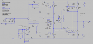
This is the EF vs Ricardo output stage (ROS for short 🙂 ).
The second image the emitter resistors of the EF have to be increase to 0.6 for matching the ROS gain, the ROS have a lower gain than the EF because is driven by a higher impedance , in terms of thermal control I think that ROS and EF may be very similar, the ROS may be more thermal stable and emitter resistors can be even lower than 0.2 for lower crossover distortion, I think that even a 0.1R will work here, but is need further testing.
Like the EF stage, in ROS also all the output, drivers and bias spreader transistors must be mounting in the same heat-sink for thermal control ..
Thanks for that analysis Sergio, as I said in my earlier post, the emitter resistors (if kept) should be lower (my estimate was, but not published I think, near 10ohm). I would have to take a look at the collector resistor, 22ohm gives a current of 600m/22=30mA or 30m*35V=1watt, not to bad, and very acceptable. But a bit higher (like 47ohm or 100ohm) will halve/quarter that power and make the ROS more temperature stable (my feeling is that a higher value may be beneficial).
One more thought, if the driver is capable of caring significant current/power, then there may be a HF danger. As the drivers are faster than the output devices they will have the tendency to deliver a part (maybe to much) of the output power (due to the fact that the output devices are slower). This situation has to be simulated (as I know from recent experience 🙁). It may be needed to simulate this behavior at frequencies up to 10Mhz (that was needed in my case).
But (most probably) not a problem with an amplifier running at +-35V. Still, as this is a learning project, needed to be mentioned.
But (most probably) not a problem with an amplifier running at +-35V. Still, as this is a learning project, needed to be mentioned.
Last edited:
If you want the most linear output stage with only on pair of power bjt the best is the EF stage without emitter resistors, the problem is that without this resistors the output stage is no longer thermal stable and the most probably outcome is that the amplifier life will be very short  .
.
But if the output stage transistors would be cascoded, and the Vce of the output transistors would be something like 3 v , I think that in those conditions the stage would be thermal stable, it could be tried ... It may work 😉.
.But if the output stage transistors would be cascoded, and the Vce of the output transistors would be something like 3 v , I think that in those conditions the stage would be thermal stable, it could be tried ... It may work 😉.
Attachments
If you want the most linear output stage with only on pair of power bjt the best is the EF stage without emitter resistors, the problem is that without this resistors the output stage is no longer thermal stable and the most probably outcome is that the amplifier life will be very short
But if the output stage transistors would be cascoded, and the Vce of the output transistors would be something like 3 v , I think that in those conditions the stage would be thermal stable, it could be tried ... It may work 😉.
That's a cool thought. I have an other one, you could (actually as I did) have a Mosfet in series with a BJT (thermal wise) and so stabilize the bias 🙂
Can you draw me a picture Frans 😕
Sorry, bot no I can not, maybe on a later date.

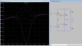
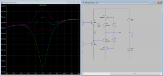
the problem is that I do not know what this curve, you have an explanation?
what is a good curve ?
I only sim THD20K 0.002% to 0.005% 1W/100W
what is a good curve ?
I only sim THD20K 0.002% to 0.005% 1W/100W
The best curve is a straight line 🙂 , the less stepper the line are, the better, a graph with stepper up´s and down´s indicates that the crossover distortion will be worst and difficult to get rid of that distortion by feedback, as the harmonics will spread higher in frequency. Your circuit is a CFP so the curve will be very stepper at the crossover region (around zero).
Sorry, bot no I can not, maybe on a later date.
Ok, will wait.
Have to go now.
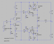
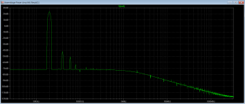
After much reading and simulating I decided to let go the driver emitter's resistors, increase a little bit idling current and also lower the driver's base stoppers.
FFT looks increasingly good.
Please have a look at the simulation.
Unless I get an objection from any of you I will start populating.
Already have the boards....
FFT looks increasingly good.
Please have a look at the simulation.
Unless I get an objection from any of you I will start populating.
Already have the boards....
Attachments
Ricardo, you can not do that. Read the Rod Elliott page about a similar output stage, see where the resistors are in the output stage.
60-80W Power Amplifier
60-80W Power Amplifier
After much reading and simulating I decided to let go the driver emitter's resistors, increase a little bit idling current and also lower the driver's base stoppers.
FFT looks increasingly good.
Please have a look at the simulation.
Unless I get an objection from any of you I will start populating.
Already have the boards....
This is not a good idea, for one there will be a thermal risk. I would advice you to do some thermal simulations.
if you replace the input BJT with a cascoded Jfet you have the option of making it DC coupled-- here is an old version of mine.
For more OPS pairs I would strongly suggest emitter resistors. for two pairs 0,22 Ohm will do. Also CFP OPS with more output pairs are known to be troublesome.
EF3 would be a better choice or for simplicity lateral Fet's driven directly from your VAS would be a strong choice
For more OPS pairs I would strongly suggest emitter resistors. for two pairs 0,22 Ohm will do. Also CFP OPS with more output pairs are known to be troublesome.
EF3 would be a better choice or for simplicity lateral Fet's driven directly from your VAS would be a strong choice
Attachments
Last edited:
Ricardo, you can not do that. Read the Rod Elliott page about a similar output stage, see where the resistors are in the output stage.
60-80W Power Amplifier
Hi Sergio
You mean The collector resistors between the output trannies ?
Will sim it your way 🙂
if you replace the input BJT with a cascoded Jfet you have the option of making it DC coupled-- here is an old version of mine.
For more OPS pairs I would strongly suggest emitter resistors. for two pairs 0,22 Ohm will do. Also CFP OPS with more output pairs are known to be troublesome.
EF3 would be a better choice or for simplicity lateral Fet's driven directly from your VAS would be a strong choice
Hello Miib
Thank you for your input.
I like your input stage and appreciate the critical comments but need some leverage (What is the EF3 OPS ?)
EF3 is three emitter followers, see the CFA rumble thread, there Ostripper has a well tested OPS.
For your circuit I would opt for Lat fets, They are easy to drive directly of the VAS with app 5 mA/pair, so if you have 10 mA running over your bias-spreader you can have two pairs.
For your circuit I would opt for Lat fets, They are easy to drive directly of the VAS with app 5 mA/pair, so if you have 10 mA running over your bias-spreader you can have two pairs.
EF3 is three emitter followers, see the CFA rumble thread, there Ostripper has a well tested OPS.
For your circuit I would opt for Lat fets, They are easy to drive directly of the VAS with app 5 mA/pair, so if you have 10 mA running over your bias-spreader you can have two pairs.
Would you care to post a simple schematic ?
- Home
- Amplifiers
- Solid State
- Assemblage Power Amp