Wavebourn, have you ever tried the hydrochloric acid + hydrogen peroxide etching method? It works very well and is very clean, the solution turns a clear green with no sludge.
Did a long time ago when did not have a ferric chloride. Also, "Root Killer" with a kitchen salt 1:1 works well enough. Nitric acid works fast, but it is dangerous.
Novermind, I expect my ferric chloride soon by UPS Ground.
I got it, finally, more than a month after ordering... 2 lbs of a powder, that means 1 gallon of a water. It heats up significantly being dissolved, so I need to pour it slowly into water mixing carefully by some plastic thing... I am going to dissolve all of it at once and keep in a glass container because left in bag remains will absorb water from an air and damage a polyethylene bag.

I dissolved it in a plastic bucket with 1 gallon of cold water with an ice in it. At the end water was almost boiling. I expect no more than 5 minutes to etch the board that was drawn August, 14!
We're watching 🙂
Thanks; I'll post a picture of the board. I'll go check now, most probably it is ready.
The board is etched. I washed it thoroughly with a soap in a warm running water, going to clean by acetone to remove protective paint, then lightly sand it by #240 paper before soldering.
It is ready for soldering now. Let me remind what it is: it contains a small control power supply, a power on relay, servos for output stages, and speaker protection against DC in case of some emergency.

Well, I had to take a break from this project and from forum activity since got a contract in Unix administration field; now the contract is over so I am back here. I have to recall all details of the project in order to continue it... but I am hungry! 😀
Enjoy. Since it is public domain already... 🙂

I see the version you post here has a bjt, I have some of your schematics made with fets, but then as I want use a 12ax7 the capacity plays a big role, bjt has less capacity, and are better in the low current triodes.
al the tests I did, differenty are most though the used power mosfets, therefore I go test a compound stage.
In the last breadboard I used 6N1P input loaded on BSP-225 P-type MOSFET, and triode strapped 6P15P loaded on IRF730. Pictures on oscilloscope you could see in this thread belong to this version, except one when I tried 6N2P (close to 12AX7) resulted in too asymmetrical phase distortions on high frequencies than I would accept.
I still did not finish building the prototype...
I still did not finish building the prototype...
In the last breadboard I used 6N1P input loaded on BSP-225 P-type MOSFET, and triode strapped 6P15P loaded on IRF730. Pictures on oscilloscope you could see in this thread belong to this version, except one when I tried 6N2P (close to 12AX7) resulted in too asymmetrical phase distortions on high frequencies than I would accept.
I still did not finish building the prototype...
12ax7 works best in Mu-stage with penthode on top, then sound is very open with details, tube has then enormous headroom because of the high plate impedance with penthode ccs on top.
mosfets works fine with higher current tubes, today I get 6N9C tubes from russia, and earlier 6N2P and 6N1P are coming together with 6AS7.
6P15P are good for a mu stage.
so I can do a polka soon.
Last edited:
Well, I had to take a break from this project and from forum activity since got a contract in Unix administration field; now the contract is over so I am back here. I have to recall all details of the project in order to continue it... but I am hungry! 😀
Hopefully you have not sent all your knowledge to /dev/null, haven't you?
Hopefully you have not sent all your knowledge to /dev/null, haven't you?
Do not wait!

Member
Joined 2009
Paid Member
Wavebourn,
Referring to the schematic in post1 - why don't you drive the gate of the FET from the emitter of the transistor Q7 for a low impedance drive ?
Do you still favour this output stage design, or do you have a better one (and would you share it) ?
Referring to the schematic in post1 - why don't you drive the gate of the FET from the emitter of the transistor Q7 for a low impedance drive ?
Do you still favour this output stage design, or do you have a better one (and would you share it) ?
Wavebourn,
Referring to the schematic in post1 - why don't you drive the gate of the FET from the emitter of the transistor Q7 for a low impedance drive ?
Do you still favour this output stage design, or do you have a better one (and would you share it) ?
Q7 is a voltage to current converter. Collector current reflects voltage drop change on the plain linear resistor in emitter. If we add there some capacitance, especially non-linear one, can you imagine what happens?
The main idea was, to load a source follower on a counter-modulated current source.
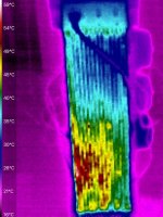
Better ideas? Yes! There was one, when a source follower was bootstrapped by another one. So called "Augmented source follower" loaded on counter-modulated current source. It was real room heated, and I never finished the prototype, it still lives in the corner of my living room. 🙂
Member
Joined 2009
Paid Member
Thanks - explains perfectly. I like your approach (this also gives me further insight into so-called JLH Follower at the same time). I didn't see new designs from you for awhile, not sure if because the old ones are still unbeaten, your are too busy, or they are not public domain.
Last edited:
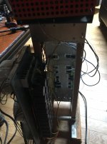
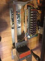
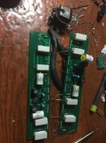
Time for the next version, improved... It will be 100W per channel now. BJT CCS, Sic MOSFET augmented source followers. PCBs for output stages.
Attachments
Member
Joined 2009
Paid Member
Wavebourn,
In the spirit of using what is in the parts bin.......Is it possible to achieve good results from this design with all-BJT output. In other words, instead of FET at the output, use a darlington BJT (to ensure sufficiently high impedance load on the driver stage) made from discrete darlington based on 2N3055 for the final power output ?
Actually, I have heatsinks with total of 16 2N3055's literally riveted to the heatsinks - and I only need single channel mono amp. I could use another 2N3055 to augment the follower, and another 2N3055 could be used to regulate the power rail. And leave a few 2N3055 on the heatsink as spares.
Last edited:
Time for the next version, improved... It will be 100W per channel now. BJT CCS, Sic MOSFET augmented source followers. PCBs for output stages.
How does the SIC mosfets into such amp? have these not a big gate capacitance or other beefy drive needs?.
I did a full platefollower version, people here did like the sound very much, really fast but still soft sound.
regards
Attachments

Last edited:
Member
Joined 2009
Paid Member
- Home
- Amplifiers
- Tubes / Valves
- Wavebourn Tower-III High-end hybrid amp