The solution is easy: litz wire or foil
Pack, Feindrhte, GmbH, HF-Litzen, Litzen Feindraht, Feindrhte aus Kupfer und Aluminium
Pack, Feindrhte, GmbH, HF-Litzen, Litzen Feindraht, Feindrhte aus Kupfer und Aluminium
Tip#10 Reducing copper loss at high frequency
For a given frequency, electrons has the bad habit to travel near of wire surface, this is known as Skin effect.
The skin depth δ, is thus defined as the depth below the surface of the conductor at which the current density has fallen to 1/e
δ ≈ √(2 ρ / μ ω)
Where
δ is the skin depth [δ]=mm
ρ = 0.017 (Ω mm2) / m , copper resistivity.
μ ≈ 1 is the magnetic permeability of copper [μ]=dimensionless
ω = 2 π f
At 100KHz, for copper, δ≈0.23mm
Then do not make sense to use too thick wires.
The solution is easy: litz wire or foil
This is easy when few number of turns are requiered, as in many SMPS's, but large number of turns go to a high winding capacitance. :-D
There is a second effect, perhaps less known, and is proxi effect (proximity), well understood reading the TI application notes by Lloyd Dixon, and related to the Dowell Curves,m very usefull designing SMPS tranformers and inductors.
Last edited:
The solution is easy: litz wire or foil
Pack, Feindrhte, GmbH, HF-Litzen, Litzen Feindraht, Feindrhte aus Kupfer und Aluminium
We are talking about secondary windings, where thicker wire are needed, and that is exactly the idea, lucky you, here Litz wire was common on mi childhood, even in my town on the middle of nothing, now is almost impossible to obtain.
On the other hand, capacitance would increase unless you use the right litz wire, so my approach is to make winding interleaving with many secondaries with as less layers as possible, all paralleled, this allow the use of thinner single wire without compromising copper losses, and the most important, this is cheap.
Be in mind that secondary shunt capacitance will be reflected to the primary, always do the math to choose the best approach.
This is easy when few number of turns are requiered, as in many SMPS's, but large number of turns go to a high winding capacitance. :-D
Agree, but out there, can be obtained some special Litz wire with less wires and thicker insulation, all depends on each particular case.
There is a second effect, perhaps less known, and is proxi effect (proximity), well understood reading the TI application notes by Lloyd Dixon, and related to the Dowell Curves,m very usefull designing SMPS tranformers and inductors.
Proximity effect can be mitigated increasing insulation thickness between primary and secondary, it is supposed already done, to decrease interwinding capacitance.
Proximity effect has great impact on SMPS transformers, where you must transfer energy at a single high frequency, say in the order of 100 KHz, however in audio OPT at about 500 Hz core losses are becoming to be high, and above in the order of, say about 5 KHz is as if you have not a core anymore.
Tip#10 was intended mostly to avoid the use of enormous wires "al pedo" (for nothing) 😀
Proximity effect can be mitigated increasing insulation thickness between primary and secondary
No, Negro. Proxy effect is caused by electromagnetic field of one conductor to another, like the skin effect, but in the neighbour one, be it of the same coil or another in the same core. The only way to reduce it is cancelling NI between primary and secondary/es, interleaving them. Also, proxy effects increases with the # of layers, squeared. By this reason, most switching transformer has a long tongue relative to the tongue diameter, so the coil is large, but has low number of layers, the lower, the best in this aspect.
"...wires "al pedo" (for nothing)" Not a good translation‼... :-D
Last edited:

You too Brutus...🙄
Warn you that right now I am without medication, also you ruined my nap... again, so I can pass so quickly to fight-mode. 😀
Mind you that electromagnetic field intensity due to a current flowing on a conductor goes as 1/r², from there its name "proximity effect" and the root of the problem, then you can reduce it increasing the distance between conductors.
Interleaving is the best way to do that, but mind you that, in a properly designed OPT, interleaving is a must, so it was already assumed, then you only can increase the distance between primary and secondary windings.
As discussion about language has become common on this thread, I should have said "between primaries and secondaries"
Happy? 🙄
Hey, that's the most accurate translation, literal translation would be both insulting and less accurate, almost incomprehensible.
More datails here 😀
http://www.diyaudio.com/forums/lounge/213901-silly-questions-answers-3.html#post3049700
Warn you that right now I am without medication, also you ruined my nap... again, so I can pass so quickly to fight-mode. 😀
No, Negro. Proxy effect is caused by electromagnetic field of one conductor to another, like the skin effect, but in the neighbour one, be it of the same coil or another in the same core. The only way to reduce it is cancelling NI between primary and secondary/es, interleaving them. Also, proxy effects increases with the # of layers, squeared. By this reason, most switching transformer has a long tongue relative to the tongue diameter, so the coil is large, but has low number of layers, the lower, the best in this aspect.
Mind you that electromagnetic field intensity due to a current flowing on a conductor goes as 1/r², from there its name "proximity effect" and the root of the problem, then you can reduce it increasing the distance between conductors.
Interleaving is the best way to do that, but mind you that, in a properly designed OPT, interleaving is a must, so it was already assumed, then you only can increase the distance between primary and secondary windings.
As discussion about language has become common on this thread, I should have said "between primaries and secondaries"
Happy? 🙄
"...wires "al pedo" (for nothing)" Not a good translation‼... :-D
Hey, that's the most accurate translation, literal translation would be both insulting and less accurate, almost incomprehensible.
More datails here 😀
http://www.diyaudio.com/forums/lounge/213901-silly-questions-answers-3.html#post3049700
Last edited:
Switching transformers and output transformer, have some things in common:
1.- They are both, transformers :-D (no one is autotransformer, who has it own peculiarities).
2.- They MUST pass high frequencies, SMPS must pass the high slew rate of the rectangular waves for a fast commutation, in audio to support the higher order harmonics.
3.- They MUST pass power from one side to other (Except in Boost topologies and its derivatives, the energy storage in the core is inconvenient and undesirable.).
4.- As many times audio transformers are involved in NFB, switching almost always, its response at closed loop MUST be good for proper performances.
5.- Usually, the have relatively larger turns ratios.
6.- Both of them MUST have low leakage inductances and low inter and intra winding capacitances.
7.- They have large voltage differences between primary and secondary/ies, so good isolation is mandatory.
The main difference is the core size and material. So, I am sure all that makes a good switching transformer, must work well for an audio one, and vice-versa.
Only for audio units, the low frequency response is important, SMPS counterparts don't take advantage in this point.
Please, continue teaching us, professor‼
Last edited:
No, you are confused, or I strongly disagree or whatever...no, just kidding. 😀
Not necessarily.
If you do that with an audio OPT, shunt capacitance will be sky high, because of core size, unless you use vertical sectioning.
So, I am sure all that makes a good switching transformer, must work well for an audio one, and vice-versa.
Not necessarily.
By this reason, most switching transformer has a long tongue relative to the tongue diameter, so the coil is large, but has low number of layers, the lower, the best in this aspect.
If you do that with an audio OPT, shunt capacitance will be sky high, because of core size, unless you use vertical sectioning.
Last edited:
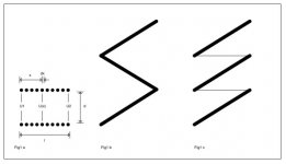
Tip#11 Z Winding
As we seen before, capacitance between two adjacent layers, each one supposed as an equipotential surface, is given by
Where
ε = Dielectric constant of insulator [cgs] dimensionless
A = Average winding area [cm²]
d = Insulator thickness [cm]
[C] = cm, 1cm ≈ 1.113 pF (cgs units are better!)

Suppose now two adjacent layers as seen on Fig1 a, the voltage difference at a point x can be written as
The capacitance of a small element of wide dx and long lm is
The energy stored into this capacitance element is
Then
Or
Referred to a voltage U, we can write
Then, the capacitance between two adjacent layers is
For the special case where the voltage between layers is uniform, U1=U2
For the usual U winding as seen on Fig1 b, the capacitance between two adjacent layers, when U1=0, U2=2U/N, from (*)
Where N is the number of layers in a winding, then the capacitance of the whole winding is
Or
Nothing new, but for the special case of Z windings, as seen in Fig1 c, U2=U/N, then, capacitance between two adjacent layers, from (**)
Then
Or
Then Z winding has 75% of the U winding capacitance, not to uncork champagne...🙄
Conclusion: Too much work almost "al pedo" (for nothing). 😀
As we seen before, capacitance between two adjacent layers, each one supposed as an equipotential surface, is given by
Cl ≈ (ε A) / (4πd)
Where
ε = Dielectric constant of insulator [cgs] dimensionless
A = Average winding area [cm²]
d = Insulator thickness [cm]
[C] = cm, 1cm ≈ 1.113 pF (cgs units are better!)
Suppose now two adjacent layers as seen on Fig1 a, the voltage difference at a point x can be written as
U(x) = U1 + (U2-U1) (x/l)
The capacitance of a small element of wide dx and long lm is
dC ≈ [(ε lm) / (4πd)] dx
The energy stored into this capacitance element is
dℇ = (1/2) U²(x) dC = (1/2) [(ε lm) / (4πd)] [U1 + (U2-U1) (x/l)]² dx
Then
ℇ = ∫dℇ = (1/2) [(ε lm) / (4πd)] (l/3) [(U1)²+U1U2+(U2)²]
Or
ℇ = (1/6) [(ε A) / (4πd)] [(U1)²+U1U2+(U2)²] = (1/6) [(U1)²+U1U2+(U2)²] Cl
Referred to a voltage U, we can write
ℇ = (1/2) Ce U²
Then, the capacitance between two adjacent layers is
Ce = [(U1)²+U1U2+(U2)²] Cl / (3 U²) (*)
For the special case where the voltage between layers is uniform, U1=U2
Ce = (U2)² Cl / U² (**)
For the usual U winding as seen on Fig1 b, the capacitance between two adjacent layers, when U1=0, U2=2U/N, from (*)
Ce = 4 Cl / (3 N²)
Where N is the number of layers in a winding, then the capacitance of the whole winding is
Ctotal = 4 (N -1) Cl / (3 N²)
Or
Ctotal = (4/3N) [1 - (1/N)] Cl
Nothing new, but for the special case of Z windings, as seen in Fig1 c, U2=U/N, then, capacitance between two adjacent layers, from (**)
Ce = Cl / N²
Then
Ctotal = (N -1) Cl / N²
Or
Ctotal = N [1 - (1/N)] Cl
Then Z winding has 75% of the U winding capacitance, not to uncork champagne...🙄
Conclusion: Too much work almost "al pedo" (for nothing). 😀
Attachments
Last edited:
Ctotal = N [1 - (1/N)] Cl
Damn! I am confused, and I strongly disagree ! 😀
Ctotal = (1/N) [1 - (1/N)] Cl
That is ! 😉
That is ! 😉
"to much work"
I strongly disagree!
With a normal winding machine it can be done in just 1 minuut extra time.
I strongly disagree!
With a normal winding machine it can be done in just 1 minuut extra time.
Damn! I am confused, and I strongly disagree ! 😀
I believe you are not well... The smell to your fried brain can be feel up to 1000Km distance.
"to much work"
I strongly disagree!
With a normal winding machine it can be done in just 1 minuut extra time.
Hand wound, it could be done by me in just one extra month... 😀
Each time a wire crosses over each layer in the winding, a small bump formed, after N layers it became horrible, even more, it changes the direction of the fields, making them less homogeneous, unless you connect each layer outside the winding, anyway, a little bit thicker insulation between layers is more effective in order to reduce winding capacitance, e.g. 0.05 mm reduces interlayer capacitance by a factor 2, I mean passing from 0.05 mm of wire enamel, to a total of 0.1 mm. 😉
I believe you are not well... The smell to your fried brain can be feel up to 1000Km distance.
No, you are confused, I strongly disagree! 😀
That minor detail, N instead 1/N, was due to I was almost asleep. 😀
Last edited:
No, you are confused, I strongly disagree! 😀
You strongly disagree yourself???
Mmmm, you are at the oven, with potatoes!
The old DOS Tango PCB, the grandfather of Altium Designer, is great to design PCBs, not to make other drawings, so the idea was to apply linear superposition principle to make simpler drawings, after all, physics doesn't change.
Emails from my friend Martin, and a long discussion with my friend Osvaldo, convinced me that my drawings are confusing. 🙄
His point was clear and overwhelming: most people are accustomed to see drawings representing reality in "real time", i.e. AFTER the vectorial sum that requires linear superposition principle, then my drawings seems bizarre and confusing.
So, I downloaded a program to make reasonably good drawings.
On post#234 has been roughly showed with numbers a guess made on post#231, and as I said before, an image worth a thousand words, mine worth only a hundred...sometimes less. 😀

The constancy of μ(AC) over a loop is a necessary condition to linearity, indeed, other approaches, as constancy of Lp, or magnetizing current behavior are equivalents.
Note1: DC magnetic hysteresis curve Bdc=f(Hdc) for each example, are drawn in order to not superimpose both loops.
Note 2: I strongly refuse to make another drawing. 😀
Emails from my friend Martin, and a long discussion with my friend Osvaldo, convinced me that my drawings are confusing. 🙄
His point was clear and overwhelming: most people are accustomed to see drawings representing reality in "real time", i.e. AFTER the vectorial sum that requires linear superposition principle, then my drawings seems bizarre and confusing.
So, I downloaded a program to make reasonably good drawings.
On post#234 has been roughly showed with numbers a guess made on post#231, and as I said before, an image worth a thousand words, mine worth only a hundred...sometimes less. 😀
The constancy of μ(AC) over a loop is a necessary condition to linearity, indeed, other approaches, as constancy of Lp, or magnetizing current behavior are equivalents.
Note1: DC magnetic hysteresis curve Bdc=f(Hdc) for each example, are drawn in order to not superimpose both loops.
Note 2: I strongly refuse to make another drawing. 😀
Attachments

Bingo!
A page that illustrates the point better than me, and with real pictures!
I guess that such qualitative measurements was made at about 50Hz/60Hz, however is a very good and clear description.
http://ttradio.net/images/tubetrx.htm
Tamura F-2013 specs, here
TAMURA CORPORATION - Transformers
More specs and sizes, here
Tamura output transformers OPT main page
Being a potted transformer, and doing by myself potted transformers with flexible epoxy, my guess for core size is that it is an EI 120/40 or something similar.
Last edited:
my guess for core size is that it is an EI 120/40 or something similar.
Sorry, my guess is wrong, because that particular transformer uses a cut C core.
http://www.tamura-ss.co.jp/en/electronics/trance08/pdf/f2010-2000-4_6_700.pdf
Anyway, core size should be similar.
BTW, Japanese drawings are not far better than mine. 😀
Last edited:
poppilin, thank you for the links, very informative...
You're welcome, Tony.
Seems that them finally show what I have been saying, isn't it? 😎
BTW, I am working on an equation that answer your question on how big a core must be, letting aside the art, of course... 😀
Tip#12 Core Area
Let's consider maximum values for the fields B and H
Effective power must be
Then, minimum needed core area will be
Multiplying and dividing by μ on both members
For the vilified transformer of post#71
Using the rule of dumb of post#2
Naturally this value is overestimated, as all rule of dumb is supposed to work.
Note: Just in case, to avoid future claims, let's clear that on a gapped core, we must take μ as its effective value
Let's consider maximum values for the fields B and H
Bac(max) = (Uac x 10⁸) / (√2 π fo S Np)
Hac(max) = (4 √2 π Np iac) / (9 l)
Hac(max) = (4 √2 π Np iac) / (9 l)
Effective power must be
P = η Uac iac = (9/4) η fo S l Bac Hac x 10⁻⁸
Then, minimum needed core area will be
S = (4 P x 10⁸) / (9 η fo l Bac Hac)
Multiplying and dividing by μ on both members
S = (4 μ P x 10⁸) / (9 η fo l Bac²)
For the vilified transformer of post#71
S ≈ 10.8 cm²
Using the rule of dumb of post#2
S = 1500 √(P / fo Bmax) ≈ 11.9 cm²
Naturally this value is overestimated, as all rule of dumb is supposed to work.
Note: Just in case, to avoid future claims, let's clear that on a gapped core, we must take μ as its effective value
μeff = l μ / (l + lG μ)
Last edited:
You're welcome, Tony.
Seems that them finally show what I have been saying, isn't it? 😎
BTW, I am working on an equation that answer your question on how big a core must be, letting aside the art, of course... 😀
what i do is compute for the 60hz power capacity and scale it down to say 20hz...so that if a core can do 300 watts at 60hz then is is probably good for 100 watts at 20 hz....i know this is too simplistic but it is a start, maybe you can investigate further....😀
- Status
- Not open for further replies.
- Home
- Amplifiers
- Tubes / Valves
- Design of transformers for valve amplifiers