LOL, I paid for a mint condition NOS one on eBay just this morning, I should have it in a few days.
I wonder the same, so I decided to give one a try.
ADC is AKM5393, and DAC is AKM4393.
I have found discussion on the net of the usual Behringer 'ímprovements', but so far no real measurements.
I have an Edirol UA-25ex usb soundcard with spdif in/out.
Hopefully with the Edirol, the SRC2496 effectively becomes a usb soundcard, better than the Edirol.
The Edirol ADC kicks up truckloads of harmonics at input levels greater than about -6dBfs.
So, in combination with AWA F242 D&N set used as auto nulling notch filter, maybe I end up with pretty good loopback testing with any T&M software, unlike the QA400.
The SRC has a front panel stereo input level control.....total pita.
That might get replaced with stepped attenuators or 10-turn trimmers for accuracy, stability and set-ability.
Mods/improvements suggestions are welcome.
Dan.
This should be interesting.
I have one still in a box from last year's bright idea dept.
What is the AWA thing look like and cost?
THx-RNMarsh
Maybe you can send them back and ask to plate the holes... if a mistake... no cost to you.... if they said you didnt ask for plated thru holes... its a few coins extra. Thats what i would do.
-RNM
Richard the plating is done before etching the board. The holes are drilled first, plated and then the resist is put on the board. It's not possible to have them plated after the fact. All double sided boards are plated, You can't have them done without plating as an option. OSHPark adds your order to a panel with 300 other orders on the panel. That means none of the boards on the panel where plated. The gold plating on the surface is there but nothing on the walls of the holes. Just bare FR4.
The board house screwed up.
As long as its not multi-layer you can stick wires and solder on both sides. That's 1960's tech. I would do one to see if there are other mistakes to fix but never two and never for something that needs to be reliable.
As long as its not multi-layer you can stick wires and solder on both sides. That's 1960's tech. I would do one to see if there are other mistakes to fix but never two and never for something that needs to be reliable.
This is what I'm doing at the moment. Mostly because I have a week off and wanted to get this done. This is a proto and undoubtedly there will be changes. I paid for through hole plating. That's why I stopped making boards. OSHPark's minimum is three as you know.
I think they will fix the problem nut it will be another month. WOW 300 boards. Hate to be in there position.
This should be interesting.
I have one still in a box from last year's bright idea dept.
What is the AWA thing look like and cost?
THx-RNMarsh

The AWA is an Aus built 80's D&N set.... auto nulling makes life so much easier.
The going price is around $250.00 or so .....if you can find one that is !.
The companion super low distortion generator is the AWA G232.....if anybody knows of one for sale, please let me know.
http://isurplus.com.au/manuals/AWA%20F242A%20User%20Manual.pdf
Dan.
Edit: I just arranged 20 medical grade 240V 225VA isolation transformers for $10.00 each....these will come in very handy.
Attachments
Last edited:
It certainly sounds like a screw-up by the etch and drill house - but it would almost have to be a double screw-up, since I'd expect an electrical test to detect the lack of continuity between top and bottom layers. Before you scream too loud, take a very careful look at the fab files you submitted. In fact, a second set of eyes might be a better choice for the second look.Just got my PCB from OSHPark this week. Part way through assembling one of them I discovered there is no plating on any of the pad holes or vias. This is a double sided board and quite useless without plated holes.
Anyone seen this before.
- CAD operators have been known to suffer from a short-circuit between the headsets, causing them to look cross-eyed at the menus for building pad stacks in their PWB layout software, and select the check box for "Non-Plated Thru Holes" (NPTH) rather than PTH. That doesn't really explain why it should affect EVERY pad and via on the PWB, unless it was done by accident when somebody made a "minor" global change, such as adjusting the solder-mask swell or paste-stencil shrink.
- Some hobbyists have tried to make PWB layout software more friendly to home fabricators by placing a dimple or divot in the center of every pad. The intent is that it will be an aiming-point and guide for manual drilling. This can be disastrous in an automated etch-and-drill process if this hole in the copper (only) is interpreted as taking precedence over the hole specified in the pad stack.
Dale
It certainly sounds like a screw-up by the etch and drill house - but it would almost have to be a double screw-up, since I'd expect an electrical test to detect the lack of continuity between top and bottom layers. Before you scream too loud, take a very careful look at the fab files you submitted. In fact, a second set of eyes might be a better choice for the second look.
(And in exchange for a serving of my favorite malt beverage, the guilty party can rest assured that neither co-worker nor supervisor will ever learn of such a slip-up from me. The clerk in Configuration Management who maintains the Drawing Change logs, however, may not be so easily persuaded.)
- CAD operators have been known to suffer from a short-circuit between the headsets, causing them to look cross-eyed at the menus for building pad stacks in their PWB layout software, and select the check box for "Non-Plated Thru Holes" (NPTH) rather than PTH. That doesn't really explain why it should affect EVERY pad and via on the PWB, unless it was done by accident when somebody made a "minor" global change, such as adjusting the solder-mask swell or paste-stencil shrink.
- Some hobbyists have tried to make PWB layout software more friendly to home fabricators by placing a dimple or divot in the center of every pad. The intent is that it will be an aiming-point and guide for manual drilling. This can be disastrous in an automated etch-and-drill process if this hole in the copper (only) is interpreted as taking precedence over the hole specified in the pad stack.
Dale
The thought has crossed my mind - was it something I did. I used the defaults in DipTrace.
I don't recall doing anything different. I sent gebers out to three different board houses internationally including OSHPark and have never encountered a problem before. The last set of boards from OshPark were flawless except for the solder mask color but that's a matter of opinion. I don't know how it would be controlled for a panel of 300 to plate some boards but not all. Surely anyone doing a SMT board at some point needs to use a via. So either the whole batch is screwed or I've got really bad luck. Doesn't make me want to use them again. We'll see how it turns out.
I had a batch of 40 boards done many years ago. The board house printed the boards reverse side from the art work. They were good enough to claim the error and printed a new set.
The board without through holes plating turned out fine. Just took a very long time to assemble. OshPark issued an refund no questioned asked but suggested pilot holes may be turned on.
Isolation from USB really does work well. Have full USB control of my oscillator without even a spec showing up on fft.
Isolation from USB really does work well. Have full USB control of my oscillator without even a spec showing up on fft.
Attachments
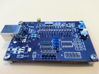
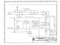
That looks like a USB to GPIO interface. I don't see the oscillator there. Nicely done. Are you creating the software as well?
That looks like a USB to GPIO interface. I don't see the oscillator there. Nicely done. Are you creating the software as well?
It's an isolated GPIO. The controller isn't on the board as shown. That's what all the socket pins are for. Right behind the socket pins is a 20 MHz crystal. Soldering all those pins on both sides was a real chore. But that's what you have to do if there's no plating. There are two isolators which share an SPI port the other ports are for CS or GPIO. One SPI port is assigned to the oscillator and the other for future use. The tuning DACs on the oscillator board are SPI and I used an SPI expander IC to drive the tuning relays. Microchip has an expander which sinks/sources 25mA per pin. Enough to drive a small relay. It's a two wire SPI with one CS to rroute the SPI clock and data line. I can send control data anywhere. The other isolated SPI port will be for the output buffer and attenuation board. Isolated analog is returned to the uPcontroller via a current loop using the IL300. This provides a signal to the uP ADC for level readout. The Software is done. Modified from microchip's demo library. There is also an isolated 1Hz res frequency counter so you know where your tuning is at.
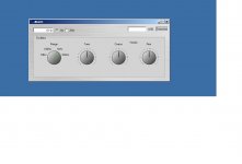
Here's what the UI looks like. More will be added as the project develops.
With the dac tuning I can add slow sweeps and auto tuning.
Using SPI means the oscillator is not married to any one micro controller. Any uP can be used. A PCI that handles SPI is an option as well.
Attachments
Last edited:
Yeah, I use Pad2Pad. Never had a problem. Really nice boards.
Thanks Dirkwright.
I own a license for Diptrace. It's good package. Much easier to learn than Eagle. It's not the software. I might have clicked on something and not noticed. I had numerous boards done from this software and never a problem.
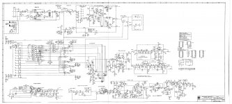
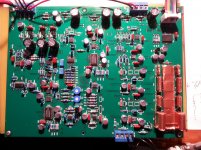
Here a shot of the oscillator.
The Mdacs haven't been mounted on this pic.
Sweet!
Samuel
Super Osc. -
Thats really, really nice!
😎🙂
-RM
Here a shot of the oscillator.
The Mdacs haven't been mounted on this pic.
Thats really, really nice!
😎🙂
-RM

Here a shot of the oscillator.
The Mdacs haven't been mounted on this pic.
Looks like you did a great job.
Thanks guys.
OSHPark identified the problem with the missing plated holes. It was my unintended fault.
I clicked on a unsuspecting check box which removed the copper underneath the drill hit.
OSHPark is back on my list with a gold star for great customer service.
OSHPark identified the problem with the missing plated holes. It was my unintended fault.
I clicked on a unsuspecting check box which removed the copper underneath the drill hit.
OSHPark is back on my list with a gold star for great customer service.
. . . OshPark issued an refund no questioned asked . . . .
So, they refunded your cost . . . then they made the effort to find, and politely show you, where YOU screwed up?OSHPark identified the problem with the missing plated holes. It was my unintended fault.
I clicked on a unsuspecting check box which removed the copper underneath the drill hit.
OSHPark is back on my list with a gold star for great customer service.
I'd say they deserve TWO gold stars!! AND a serving of their favorite malt beverage.
Regardless of which program you consider, PWB layout software is very versatile and generally includes hundreds, perhaps thousands, of options and features. But that means there are even more opportunities to make mistakes; the ways you can screw up don't increase proportionately to the number of features and options, it's more like a square or cubic power of the feature count. That doesn't even allow for the perversity of nature, or things that "just happen". As an old aphorism said,
"All the skill of the greatest marksman goes for nothing if an angel decides to pee in the pan of his flintlock."
It takes only one mistake - your fault, my fault, or nobody's fault - to render a whole batch of PWB's as scrap. Usually the PWB layout guy gets blamed, though by my estimate that's deserved only about 1/3 to 1/2 the time. The PWB layout guy (or gal - one of the better ones I've worked with was a female girl person of the opposite sex) is probably the most under-appreciated member of a product design team.
Dale
p.s. - I'm not going to take credit for making a pretty accurate prediction back in Post #966, because I'm confident that in the not-too-distant future the egg will land on MY face.
Thanks guys.
OSHPark identified the problem with the missing plated holes. It was my unintended fault.
I clicked on a unsuspecting check box which removed the copper underneath the drill hit.
OSHPark is back on my list with a gold star for great customer service.
Hmmm. I would give them a goldstar if they would inform you of the error, fixed it and send you the fixed board, rather then sending you a useless board then refund it. Seems a funny way to run a business.
jan
- Home
- Design & Build
- Equipment & Tools
- QuantAsylum QA400 and QA401