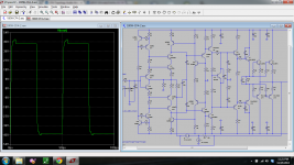
Here are the square wave plots and Loop Gain plots for both amps, MOSFET and triple BJT.
I hope it's clear from the plots what was the ULGF.
Damir
I've also simulated your BJT version schematic with square wave signal input, but the ringing looks a little different/better.
Attachments
Here are the square wave plots and Loop Gain plots for both amps, MOSFET and triple BJT.
I hope it's clear from the plots what was the ULGF.
Damir
Is the MOSFET square wave response really an issue? My VSSA cludge does the same thing and I decided to live with it. Have not built it yet but intend to.
I've also simulated your BJT version schematic with square wave signal input, but the ringing looks a little different/better.
You use input HF filter and 20kHz and mine is without filter and 100kHz.
Last edited:
Here are the square wave plots and Loop Gain plots for both amps, MOSFET and triple BJT.
I hope it's clear from the plots what was the ULGF.
Damir
Hi Dadod, your amp designs certainly demonstrated admirable distortion performances.
I started learning to use LTspice as recent as a short few months ago. Please allow a beginner's question. I found the Tian probe you have in your schematics has a backwards current source from all other people's schematic I've seen here. Perhaps the polarity wont matter in a Tian probe?
Did you have the input LPF in when you plot the square wave response? The LPF seems to have a great effect on the overshoot and ringings, as we have found with your 200W-CFA design. Perhaps a LPF can improve the overshoot and ringing here too. From my limited study into a few CFA designs it seems that despite a fast SR and a broad bandwidth, these circuit require a heavy bandwidth limit at the input in order to have a clean square wave response.
Hi Nattawa, second question is answered in my previous post.
Regarding Tian probe I noticed that voltage source direction has influence, I am not yet completely familiar with the Tian probe.
This amps were just an exercise to get distortion as low as possible, but I am not confident in it, my simpler version(200W) should be very stable and good sounding, I hope. And all the trick is in Cherry compensation.
Damir
There are many these days, you could try yourself. Mentioning brand may affecting them. You could also built your own with low few ppm buffer based or opamp based to buffer headphone for cheap solution, and hear if the buffer changes the sound.Can you name a few? What do you hear with them that isn't neutral or natural?
What does this means ?
If an amp produce no distortion, it is neutral, by definition.
If you find an amp not neutral, with real loads, this means it produce distortions, not measured with resistive loads and sinus waves.
This means we have to find other ways to measure distortions.
No there are another than just distortion, less than 0.01%THD is already perfectly unhearable.
You have a strange way to see the things ;-)No there are another than just distortion, less than 0.01%THD is already perfectly unhearable.
What else than 'distortions' can modify the "sound of a signal" and make an amplifier not 'transparent' ?
An other what ?
Which ones have you tried and what did you hear that's not neutral & natural?There are many these days, you could try yourself. Mentioning brand may affecting them. You could also built your own with low few ppm buffer based or opamp based to buffer headphone for cheap solution, and hear if the buffer changes the sound.
I don't see how mentioning the brand can change its neutrality & naturalness 🙂
Member
Joined 2009
Paid Member
Is your VFA version also a 'symmetrical' topology?
Does it have 2 parallel feedback paths?
The VFA version is also symmetrical and therefore it has two feedback paths. However, with a CFA you need a d.c. voltage difference between the two feedback nodes so each feedback path has a separate set of series R and shunt R+C. With the VFA there is no d.c. voltage between the two feedback nodes so they can share a common feedback series R and shunt R+C.
---
That JFET follower is a lovely piece of thinking.
Last edited:
The circuits I show from #1426 don't have this problem. You can even use the R4/5 to twiddle DC offset though there are better ways to do this.The VFA version is also symmetrical and therefore it has two feedback paths. However, with a CFA you need a d.c. voltage difference between the two feedback nodes so each feedback path has a separate set of series R and shunt R+C. With the VFA there is no d.c. voltage between the two feedback nodes so they can share a common feedback series R and shunt R+C.
C3/4 make the 2 feedback paths common. (V4/5 are simply to establish DC conditions quickly in sim for the THD analyzer)
You'll note I even use evil mismatched compensation 😱 on the 2 forward paths too but this certainly isn't a dominant THD mechanism.
...source direction has influence, I am not yet completely familiar with the Tian probe.
I don't see how you can reverse the polarity of the current source and still have a correct probe unless you have reversed all the associated terms in the calculation.
Have you tested this?
Best wishes
David
I don't see how you can reverse the polarity of the current source and still have a correct probe unless you have reversed all the associated terms in the calculation.
Have you tested this?
Best wishes
David
As I said I am still learning to use Tian probe. I reversed now current probe and there is a change but very small, look the plot.
BR Damir
Attachments

dadod;3717290... said:but very small, look the plot.
Your inverted probe is incorrect I think.
The difference will be small if the probe is placed after a low impedance source, here the source impedance is very low.
As the source impedance increases so will the error of the inverted probe.
Best wishes
David
Yes, I just checked that.
If the source is not low impedance then your version looks totally unusable.
Also chapeaux to Nattawa, well spotted.
Last edited:
Your inverted probe is incorrect I think.
The difference will be small if the probe is placed after a low impedance source, here the source impedance is very low.
As the source impedance increases so will the error of the inverted probe.
Best wishes
David
Yes, I just checked that.
If the source is not low impedance then your version looks totally unusable.
Thanks Dave,
This is written in LTspice LoopGain2 example:
This is an improvement over the technique shown in LoopGain.asc
because it (i) accounts for reverse feedback(it doesn't even
matter if you reverse the direction of the probe -- you still compute
the same open loop response) and (ii) the inserted probe elements
result in a smaller, sparser circuit matrix.
and I was thinking that direction of the current source does not matter.
BR Damir
...it doesn't even matter if you reverse the direction of the probe...
Very different "to reverse the direction of the probe" and to reverse the polarity of the current source within the probe, of course.
Thanks to Nattawa your tests will be more accurate.
Best wishes
David
Last edited:
Very different "to reverse the direction of the probe" and to reverse the polarity of the current source within the probe, of course.
Thanks to Nattawa your tests will be more accurate.
Best wishes
David
Yes, thanks to Nattawa and to you!
BR Damir
P.S. because of very similar result I did not notice direction error.
Last edited:
Yes, thanks to Nattawa and to you!
BR Damir
P.S. because of very similar result I did not notice direction error.
Thanks David for clarifying this. I learned from it myself.
Here are the square wave plots and Loop Gain plots for both amps, MOSFET and triple BJT.
I hope it's clear from the plots what was the ULGF.
Damir
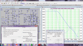
6MHz, to high for a practical implementation, this is one of those things that works in the simulator only. OTOH, using two pairs of output devices for 50W into 8ohm explains why the output stage has low distortions (only 1.8A peak for each device).
Bias the output towards the rails and determine again the gain and phase margins. You will find out why the large signal step response is not right, the phase margin will be significantly lower and the step response will overshoot.
I keep saying this, with limited success so far. CFA or VFA, there is no limit in what the loop gain can lower the distortions, as long as the ULGF is arbitrary high. For a fixed ULGF, the only possible way to increase the loop gain (for any audio amplifiers, and in general for any minimum phase system) is to increase the compensation network order. That is, inserting N poles and N-1 zeroes to bring the phase back to the Bode stability criteria.
I will also quote again the seminal work of Cherry that showed the only three way to lower distortions: increasing the bias, distortion cancellation (as e.g. in the long tail pair with current mirror load, or the Quad current dumping), and negative feedback. Anything else (like VFA vs. CFA) is a smoked mirror.
I will also quote again the seminal work of Cherry that showed the only three way to lower distortions: increasing the bias, distortion cancellation (as e.g. in the long tail pair with current mirror load, or the Quad current dumping), and negative feedback. Anything else (like VFA vs. CFA) is a smoked mirror.
Let's do more with distortion cancellation..... I would hope not to copy what others invented but invent some ways ourselves or combo circuits or integration of several ideas about cancellation techniques.
What is a basic topology for cancellation and what variations exist? We can cover what others have done to help get the creative juices flowing but would like some fresh ideas as well.
Thx-RNMarsh
Last edited:
6MHz, to high for a practical implementation, this is one of those things that works in the simulator only. OTOH, using two pairs of output devices for 50W into 8ohm explains why the output stage has low distortions (only 1.8A peak for each device).
Bias the output towards the rails and determine again the gain and phase margins. You will find out why the large signal step response is not right, the phase margin will be significantly lower and the step response will overshoot.
I keep saying this, with limited success so far. CFA or VFA, there is no limit in what the loop gain can lower the distortions, as long as the ULGF is arbitrary high. For a fixed ULGF, the only possible way to increase the loop gain (for any audio amplifiers, and in general for any minimum phase system) is to increase the compensation network order. That is, inserting N poles and N-1 zeroes to bring the phase back to the Bode stability criteria.
I will also quote again the seminal work of Cherry that showed the only three way to lower distortions: increasing the bias, distortion cancellation (as e.g. in the long tail pair with current mirror load, or the Quad current dumping), and negative feedback. Anything else (like VFA vs. CFA) is a smoked mirror.
You should look at those schematics more carefully, they are capable for over 100 W into 8 ohm with the THD20k a bit over 1 ppm.
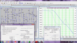
How you bias output toward the rails for .ac sim, with DC offset on input as I did in attached simulation??
If that is correct way to sim it, then I don't see a hint of instability, look attached plot. Uper output transistors are biased to 2.2 A. Maybe it is not a smoked mirror, don't be so conservative, you are young guy(student?).
BR Damir
Attachments
- Home
- Amplifiers
- Solid State
- CFA Topology Audio Amplifiers