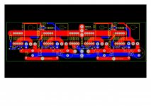
I have no 1:1 filing about dimensions but looks like ground tracks can be smaller width. Two sides can be closer in that area and rectangle will be smaller.
Thank you for the feedback. What sort of track thickness would you use for signal grounds and decoupling grounds? Currently signal = 3mm and decoupling = 4mm.
I could add a scale to the drawings if that would be useful?
Thank you for the feedback. What sort of track thickness would you use for signal grounds and decoupling grounds? Currently signal = 3mm and decoupling = 4mm.
I could add a scale to the drawings if that would be useful?
It looks bigger on first sight 🙂.
There are small currents, and it flows separately so half width will more than suffice (2mm, 1.5mm). Spacing is not critical, there is hardly potential between those tracks. Add all widths together to get effectively ground path. Top layer tracks will be shorter.
For current source stabilizing, capacitors should be connected to base of source transistor (example u3) not to ground.
Last edited:
For current source stabilizing, capacitors should be connected to base of source transistor (example u3) not to ground.
This is good news. It doesn't look to difficult to add some stabilization of this type. You mentioned using 220u // 220n for current sources. The smaller current sources run at approx 1mA and the larger 20mA. Could I get away with smaller decoupling for the 1mA sources?
I will be relaying out the PCB tomorrow eve with smaller ground tracks and additional decoupling.
Thank you
Paul
Let's see u3 example again. U5 is stabilizing current by keeping nearly constant voltage on emiter resistor r12 (0.6V-0.7V). Every fluctuation of supply voltage versus ground will cause current through base-emiter circuit of u5, which is amplified (hfe) through collector resistor r33. It rises voltage on r33 and voltage change on r12 stays very small. It is like that on ideal low frequency condition. As frequency rises parasitics rises, miller and phase shift spoils all work. That circuit electrically shakes on higher frequencies. We wanna keep stabile voltage on r12, and it will be as better as capacitance from emmiter u5 to collector u5 (base u3) is bigger, and as r6 is bigger of course. My experience is that overstabilization (r33 replaced with current source) makes sound improvements. Especially is evident on stage and 3d sound.
Thank you for the explanation of the function of the stabilization caps. These caps can be quite low voltage and hence smaller. There should only be two diode drops across them in normal operation. The only question is, is it a good idea? If you get a transistor failure you would get 2/3 rail voltage across them.
Thinking about it I'm thinking of ditching R52 and R53. Not sure they are giving any benefit.
Thinking about it I'm thinking of ditching R52 and R53. Not sure they are giving any benefit.
Last edited:
Thank you for the explanation of the function of the stabilization caps. These caps can be quite low voltage and hence smaller. There should only be two diode drops across them in normal operation. The only question is, is it a good idea? If you get a transistor failure you would get 2/3 rail voltage across them.
Thinking about it I'm thinking of ditching R52 and R53. Not sure they are giving any benefit.
I am not sure what "ditching" means, but those resistors have job to kill lc resonance too, I would live them there. There is good and bad things in every design, this one is unpredictable in case of transistor failure. I wouldn't say the caps only will be exposed. Voltage on input will rise and preamp or what is on input will be affected.
For that purpose smart zener protection can solve problem.
What ever happened to being simpler? 😉
Yes, well, errrrrrrrr......erm.... there's are no cascodes. I kept to that rule...... 🙂 and I gave up with hawksford in favour of Bonsai's solution.
PCB Update and the beginnings of Parasitics
Work continues on the creation... 😀
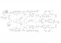
Attached are the latest schematics. Included the suggestions by overall feedback. Changed decoupling capacitors on output PCB to the ones suggested by transistormarkj. Added extra decoupling to the input PCB. There will no doubt be more changes to the PCBs to come.
Now it is time to start with the parasistics properly. Attached is the section of the circuit that I have started with. Does it look sane to do it this way. I think I'll start with the power rails and then the longer tracks.
The attachments are latest PCB layouts, schematic and the the section of the circuit I have started parasitics work on.
Work continues on the creation... 😀
Attached are the latest schematics. Included the suggestions by overall feedback. Changed decoupling capacitors on output PCB to the ones suggested by transistormarkj. Added extra decoupling to the input PCB. There will no doubt be more changes to the PCBs to come.
Now it is time to start with the parasistics properly. Attached is the section of the circuit that I have started with. Does it look sane to do it this way. I think I'll start with the power rails and then the longer tracks.
The attachments are latest PCB layouts, schematic and the the section of the circuit I have started parasitics work on.
Attachments

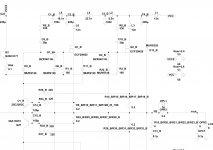

Straight away I find ringing..... There is ringing at the point where the gate snubbers connect to the positive power rail. 😀 Sweet!
Did you add ohmic parasitics?
Did you add ohmic parasitics?
I'm using figures given by gootee of 25nH per inch and 1milliohm per inch for the trace parasistics. You haven't seen the mess at the Drain of Q1_B.
I'm using square waves to excite the circuit.
I'm using figures given by gootee of 25nH per inch and 1milliohm per inch for the trace parasistics. You haven't seen the mess at the Drain of Q1_B.
I'm using square waves to excite the circuit.
The CircuitCalculator.com Blog PCB Trace Resistance Calculator
It looks little too bad, try to recalculate trace impedances.
I put a 1R+1u cap on the rails in simulation which works pretty well to stop the rail resonances that always occur when you parallel low-ESR lytics with film caps. Because the output stage is the main leakage point for rail parasitics, resonances here will push a fast amp into oscillation.
Why are you using C5171/A1930 as drivers?
You can use these discrete symbols in LTSpice to add inductances to traces without cluttering the schematic. According to Cordell's book, the gate and drain have about 5nH inductance whereas the source has around 13nH before they reach the pins, so that's a start. Just unzip them in your schematic directory or your /lib/sym directory for convenience. Then type "trace" in the symbol finder window.
Consider these calculators which may help you determine parasitics:
Wire Over Plane Inductance | Electrical Engineering Tools | EEWeb
Microstrip Impedance | Electrical Engineering Tools | EEWeb
Attachments
Keantoken,
Those trace symbols are much neater than the inductor symbol. Made some progress with the first power rail. Swapped position of two capacitors, increased the size of the film caps and added two snubbers with values you suggested. Now there are smooth changes in rail voltage rather than sharp changes with ringing.
As for the driver choice. I have an aversion to the MJE150xx devices. Too much output capacitance and slow. The A1930 / C5171 devices offered much better speed. I did go through a stage of using the A1381 / C3503 devices but then upped the driver bias (100mA) current which meant using two paralleled A1930 / C5171 devices. What do think about this? I can't decide which way to go with the driver bias.
Now plan to continue adding parasitics starting with FET parasitics.... This is going to take some time.
I agree with you about the MJE devices. However I'm not sure why the high driver bias. What does it improve?
Cbe causes BJTs to have output inductance. As Ic increases, Rm increases and the Rm*Cbe corner increases, with virtual output inductance. So we know that the two ways of decreasing output inductance of a BJT is by increasing bias and increasing Ft. Faster transistors with adequate SOA will allow you to decrease bias.
Why don't you make a dummy simulation and measure the output inductance of the drivers at various bias points against that of an inch of wire? Then you will know how many effective extra inches of wire your drivers add to your gate current loop, and whether it is important to increase bias for this reason.
If you are increasing bias to decrease the Rm (Rout) of the drivers, then you should ask whether it is significant compared to the 110R/160R gate stoppers. Rm is 26mV/100mA=260mR. 5% tolerance of 110R is 5.5, so if we set Rm at 5.5, our driver Rout can't do any worse for stability than the gate stopper resistor tolerances. 26mV/5.5R=4.7mA. You could even use bootstrapped BC550C/560C. Maybe KSC1845/A992?
I agree with you about the MJE devices. However I'm not sure why the high driver bias. What does it improve?
I have been asking myself the exact question just thinking in basic terms regarding the transistors as pure switches.
Cbe causes BJTs to have output inductance. As Ic increases, Rm increases and the Rm*Cbe corner increases, with virtual output inductance. So we know that the two ways of decreasing output inductance of a BJT is by increasing bias and increasing Ft. Faster transistors with adequate SOA will allow you to decrease bias.
I sense another brain aching session. 😉
Why don't you make a dummy simulation and measure the output inductance of the drivers at various bias points against that of an inch of wire? Then you will know how many effective extra inches of wire your drivers add to your gate current loop, and whether it is important to increase bias for this reason.
If you are increasing bias to decrease the Rm (Rout) of the drivers, then you should ask whether it is significant compared to the 110R/160R gate stoppers. Rm is 26mV/100mA=260mR. 5% tolerance of 110R is 5.5, so if we set Rm at 5.5, our driver Rout can't do any worse for stability than the gate stopper resistor tolerances. 26mV/5.5R=4.7mA.
Definitely a brain ache session. This is the kind a guidance I value. A scientific approach is best. There's not much chance I'd have figured that procedure out on my own.
You could even use bootstrapped BC550C/560C. Maybe KSC1845/A992?
An earlier experiment with LTspice was exactly that "boot strapped" drivers. Could use KSC1845/A992. I did a one time buy from mouser a while ago of all the transistors used in this design.
I have a concern about using smaller drivers. Is when the protection circuit switches in I have about 300mA flowing through the drivers. Maybe a different protection method is in order. The trouble I have is that the voltage across the TIS outputs is very low.
The parasitic work is progressing nicely. I have virtually finished the output pcb. Interesting finding was that when only the top half was done there were some strange artefacts that disappeared once the bottom half was done. Suggests layout symmetry is important. Already have some PCB changes to make even at this early stage.
Last edited:
If your drivers are bootstrapped, 300mA will pull down the bootstrap and lower the dissipation of the device. Then it becomes a matter of SOA while the Vce is falling. The BC3x7 have massive SOA so they may be a good option? Also, note that if you bootstrap drivers to the output at 12V or so, the B-C diode becomes your protection zener!
You may consider that the relationship between V, I and P is triangular. The same is true for V, I and R. Many of these electronic equations fit into a triangle or multiple connected triangles, for instance the relationship between R and power. If you try to see these triangles in everything you will see a lot of these equations are basically the same, and it will become straightforward to get from one number to the other. Try drawing the triangles on paper. You can make big pyramids. It's just sort of fun to connect distant numbers like THD and slew rate this way, and is a way of visualizing and elucidating the things you already know.
Also, look at this approach to reducing OPS parasitics:
http://www.diyaudio.com/forums/solid-state/237130-grounding-minimizing-current-loops-new-post.html
Bootstrapped drivers
Having problems with the bootstrapped drivers. I think it has exposed some sort of problem with the amp. Looks good on over load tests, GM (12dB), PM(82 degrees), sine waves, THD but not on square waves. Rising edge looks good but the falling edge overshoots (but no ringing) can solve this with a bigger cap across the feedback resistor but this seems to be a sticking plaster approach. It now has to be 1n! Don't like it.
These tests were done on the non parasitic schematic.
How would I go about tracking down the problem?
Adjust small-signal square behavior first, then increase the signal level and see what problems occur. This way you start from something reasonable.
Click on the phase scale in LTSpice and switch to group delay. Make this smooth without peaking at all output current/voltages and you will get your perfect square waves. You will notice the AC response may seem perfect but the group delay will reveal problems which will show up in the square waves.
Plot the transconductance and gain of the OPS directly and see whether it is simply the OPS producing errata at frequencies where the feedback can't clean it up. This is very hard to fix, and in simulation anyways it seems to be the worst with FET output stages.
Consider that high-slewrate amps don't necessarily have high feedback at high speeds; they just have high dynamic ability. Therefore you may achieve high slewrate but the OPS behavior must be very benign because at those speeds the feedback loop won't be able to correct many things.
Ultimately these problems are also in slow amps, the difference is that they are never observed because fast signals never escape the frontend.
- Status
- Not open for further replies.
- Home
- Amplifiers
- Solid State
- Amp design attempt number 2 (simpler)