I would switch to Cordell's 2SK1056/J162 models, since they are supposed to be similar to the Exicon parts anyway, and they are known to be close to life.
Perhaps the P-FET is much slower at the high currents at the negative excursion, and this reduces stability. Also check the beta-enhancers and diamond drivers to see if they are saturating during the square wave, and if that is the portion that overshoots. Check all stages for saturation.
A 100n or so cap across the U22/U23 emitters may improve settling time and risetime behavior.
You really should keep a basic level of parasitics in your simulation, especially when it comes time to refine RF behavior. Take your OPS out of the amp and make it stable with good frequency response and no peaking or overshoot, including full parasitics. Then add it back to the amp and readjust.
In any case, don't expect RF behavior in simulation to match real life. Play with it long enough to have an idea how to approach these problems as they show up in the prototype. Really, when you have nothing left to do but fiddle with pulse behavior, I think it is time to build the amp. Are there other aspects of the design that won't be so easily tuned once it's built? PCB layout is fixed, so have you settled on the best driver topology?
Keantoken,
Lots of things to try. Feel better having some strategies to deal with the problems. Don't like not having a plan. Just had to walk away from it last night.
I like the idea of separating the output stage and getting that right. Then I will do the same with the input stages.
The reason I did the changes on the non parasitic version was to remove those variables. Then I would transfer the changes to the parasitic version.
Could I speed up the amp (increase ULGF) to give more feedback at higher frequencies? I have found that I can get another 10 degrees PM by adding a very small capacitor parallel to the TIS emitter resistors so could safely speed the amp up while maintaining GM/PM (Don't ask me why, I do not know yet, just wanted to see the effect of this capacitor).
I'm no where near the prototype stage. Still got to complete the parasitics down to at least 5n as you suggest. I have noticed that when the amp drives a 0.1u (0.1R) load it goes into mild oscillation which it didn't without the parasitics but that's an issue for later.
I like the bootstrapped drivers. Nice neat solution and reduces component count. Not decided on bias current yet. Have had a play with simulating transistor output resistance. Had it set up in CE configuration with a DC signal (Bias). Found that after about 10mA there was no real gain from increasing bias. Going to work on this a bit more its not fully sunk in what is going on and whether I am doing things correctly.
Have decided on using the A1381/C3503 pair for the drivers. Decent dissipation and low Cob.
The plan is to then redo the PCB with the changes then back to parasitics. This is going to be an iterative process.
Thank you for helping so much with this project. I have already invested quite a bit of money in various things so it is going to happen. I'm stubborn enough....
Paul
PS. I found one of your threads from 2006 where it looks like you were just starting out. I liked the statement of one day building a good amp. 🙂
Don't worry about oscillation into capacitive loads. Simply solve it with a L/R in series with the output. The faster the amp, the smaller it needs to be. Sometimes I need no more than 180nH/8R or something like that. I would suggest leaving it at 500nH/10R for the moment as is popular. Achieve stability without load and then add the load and adjust the L/R to keep it stable. Ultimately, it is impossible to make a high-feedback amp with low output inductance and unconditional load stability at the same time. If you choose not to use the L/R, you end up emulating it through compensation tricks in the amp, with much inferior results.
Actually, my goal is to make an amp so fast that just the lead inductance of the wires to the binding posts will be enough to stabilize it. Then I can just do whatever I want. That is the holy grail, no?
Adding parasitics to the output stage before you simulate the entire amp may make the whole ordeal too complex at first. So it is helpful to establish ideal behavior first with a non-parasitic simulation.
Actually, my goal is to make an amp so fast that just the lead inductance of the wires to the binding posts will be enough to stabilize it. Then I can just do whatever I want. That is the holy grail, no?
Yes, on many fronts this is the holy grail. Everything will have to be virtually perfect to achieve that. :envy:
I'm now back at the simulator. Got the output stage separated. I think I have made a discovery. On the negative edge the U23/23 bases draw around 120mA each. Where as on the positive edge its only about 2mA.
Now going to trace the currents see where its going to.
What about C32 and C35? At transients the feedback transistors on all your current sources will be saturated, either turning off or turning full on because of the lytic bypass. 100nF should be more than enough to keep these stable. The lytics will only cause problematic recovery.
Tried removing them the lytics on the current sources. No change. It's something to do with the bootstrapping. I remove the bootstrap capacitors entirely and the current draw becomes symmetrical but 45mA.
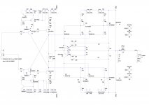
Here is what I'm simulating. I've probably made some rookie error here.
Here is what I'm simulating. I've probably made some rookie error here.
Attachments
Found biasing is failing on the negative edge. usually around 1.1V but on the negative edge hits 7V! Now the question is why. Voltage source doesn't work
Last edited:
You found a mistake they should all be 68K.
If I understand this correctly the bootstrap voltage should be quiescent voltage at the collector + whatever the output is doing.
What is very strange is that if you reverse the initial value and the Von value for the voltage source (signal generator) everything reverses and its now happening on the positive edge. The bootstrapped voltages at the collectors of the drivers is mad. One is tracking and the other seems to hit power rail + output voltage.
Its an ltspice quick. You expect the bootstrap voltage on both collectors to start off the same value (obviously one positive, one negative) but they don't. One starts off offset by the output voltage.
It's solved by using a second voltage source to give a 0V input to the amp at the start of the simulation then it runs fine. The second voltage source is a single pulse to cancel the first half cycle of the first source.
Actually, I found a way around that by using two square sources. This is the rig I use to simulate my amps. Consider it beta and incompletely documented, so ask questions if you really want to know something.
I thought it may have something to do with the bootstraps and operating point, but I didn't make the connection with the square source. This is a problem with stepped output simulations. What I do is replace the caps with voltage sources.
I thought it may have something to do with the bootstraps and operating point, but I didn't make the connection with the square source. This is a problem with stepped output simulations. What I do is replace the caps with voltage sources.
Attachments
Its a good thing in a way that you didn't make the connection. It made me think. Best way to learn. It all makes sense now and knowledge has been gained about LTspice.
It all came down to following your suggestions earlier. I now know that the output stage is benign. The exicon models are ok and that the bootstraps are fine. Thank you!
Bootstrapped drivers work a treat now 😀. This is the driver topology sorted then.
Adding voltage sources is a good way. I was thinking of adding one source to remove the offset but keeping the caps.
Shall now analyse the attachment.
Convergence at last
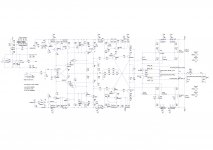
Here is what I hope to be close to the final schematic. Done a lot of experimenting and there doesn't seem to be any real improvements that can be made without significantly changing topology. Anyhow, feel I need to move on to the next stage. Which I think you can guess what that is and its not a prototype 😉
The power rail snubber positions are representative. Added VAS current limiting as I noticed during clipping the VAS was running way too much current. Lots of extreme tests have been simulated and the amp appears to be well behaved. Decided to keep the current source caps. Without them to diamond buffer current sources had a strange dip in output. Also, they don't seem to affect recovery as I think other mechanism kick in before they saturate completely.
PM = 83 degrees / GM = 12dB.
Current activity is re-laying the PCBs out. Almost complete redesign.
Attachments
Is this a current feedback amplifier?
Congratulations !
Without going into the arguments about what a CFB amplifier really is, yes.
Please hold off any congratulations until I present a scope picture... The journey still has much distance to go. But progress has been made. 😉
PM = 83 degrees / GM = 12dB.
Much better, this is around the min a allround high performance amp should have. You can use any speakers or cables without any worries.
The RC network on the bases of the vas is near always necessary to smooth a slight step that is caused by EF augmented vas in CFB. You can increase the gain margin by increasing the resistor in either the RC on the NFB compensation or the compensation of the vas but at the cost of PM. Yours is just dandy as is.
Its a nice high performance design, I would just cascode the input diamond so that I could use low noise RF transistors but your way with error correction to improve performance is a good alternate way.
Thank you. Hopefully, it'll sound good. It's up against the Leach, Sansui AU517 and Cyrus2 trio of amps.
I'm steering clear of cascodes in this version. I'm worried about cascode oscillation.
In the future there will be mk2 which I plan to try and push performance further.
Agghhhh.......The perils of parasitic simulations....
This has been a lot of work.
Have now got the all parasistics simulated down to 5n and some even below that.
THD has gone up massively and LTspice is having problems. It just spends ages source stepping.
The good news is that the circuit is stable and still has much the same spec other than thd.
If only I could get LTspice to simulate without stepping so much then I could make some progress with the THD.
Frustrating.
I hear you! That can be one of the most challenging things.
I have found on many occasions that if I leave a capacitor "dangling" with one side not connected to anything, it will stop convergence. LTSpice doesn't seem to recognize open-ended caps as singular matrixes and I'm not sure why. Deleting these caps or terminating their loose ends somehow often unfreezes the simulation. You might try Rclick->Rpar=100meg.
Also, try running the amp without solving the DC operating point (sim cmd->skip op point). This will allow you to see start-up behavior. Sometimes the sim can't find the operating point simply because the circuit in it's present state wants to latch on startup, or is unstable during startup.
"This is war".
At least its not just me. I have noticed that reducing the mosfet bias improves things. Could this be a clue?
Just tried skipping operating point and it is unstable. There's some oscillation at the beginning that dies down. Then the simulation settles down and there is no output from the amp.
At least its not just me. I have noticed that reducing the mosfet bias improves things. Could this be a clue?
Just tried skipping operating point and it is unstable. There's some oscillation at the beginning that dies down. Then the simulation settles down and there is no output from the amp.
- Status
- Not open for further replies.
- Home
- Amplifiers
- Solid State
- Amp design attempt number 2 (simpler)