Progress at last...
This has been painful....
Have found the peaking problem. I think it was always there just over looked it. Have changed the compensation of the amp and reduced the VAS current. I ended up going open loop and doing an AC analysis. The open loop response was clean but once the feedback was reconnected it reappeared. This lead me to adding a capacitor in series with a resistor across the feedback resistor. This I thought was against the rules of CFB amps. Yet, the amp smulates ok into reactive loads. The square wave output is clean. The PM is now 81 degrees and GM is 12dB. ULGF is now only 3Mhz. It could be raised but I'll leave that for real world testing. At the moment I'll stick with safety. 🙂
Have added the fly back diodes as suggested. Couldn't find a spice model for the 1N5404 so just added a MURS320 in LTspice.
The PSU is a figment of imagination at present. I envisage a dual PSU off one transformer with 30000uF + 3000uF reservoir caps. The smaller PSU will be CRCRC and the larger PSU will just be a basic arrangement. There will also be some DC protection.
All parasitics for the caps have been added back in and everything is ok.
Mark, that capacitor looks good. I especially like the ripple current. Just got to modify PCBs to accept it.
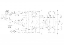
Here is the schematic...
Thank you for all your help 🙂
This has been painful....
Have found the peaking problem. I think it was always there just over looked it. Have changed the compensation of the amp and reduced the VAS current. I ended up going open loop and doing an AC analysis. The open loop response was clean but once the feedback was reconnected it reappeared. This lead me to adding a capacitor in series with a resistor across the feedback resistor. This I thought was against the rules of CFB amps. Yet, the amp smulates ok into reactive loads. The square wave output is clean. The PM is now 81 degrees and GM is 12dB. ULGF is now only 3Mhz. It could be raised but I'll leave that for real world testing. At the moment I'll stick with safety. 🙂
Have added the fly back diodes as suggested. Couldn't find a spice model for the 1N5404 so just added a MURS320 in LTspice.
The PSU is a figment of imagination at present. I envisage a dual PSU off one transformer with 30000uF + 3000uF reservoir caps. The smaller PSU will be CRCRC and the larger PSU will just be a basic arrangement. There will also be some DC protection.
All parasitics for the caps have been added back in and everything is ok.
Mark, that capacitor looks good. I especially like the ripple current. Just got to modify PCBs to accept it.
Here is the schematic...
Thank you for all your help 🙂
Attachments
Been a bit quiet of late... Been busy progressing this project.
<snipped>
1) Regarding parasitics what would be a good series resistance value for the DC supplies in LTspice? I have read that 2.6R is a good value but does this take into account the reservoir caps? If I use 2.6R I get a peaking in the closed loop response just before roll off. Not good. Can solve this by slowing the amp down but this results in an increase in THD at 20K.
<snipped>
I will be posting PCBs and updated schematics soon.
How sure are you about inserting resistance in series with the power rails?
Remember that the power rails ARE the signal path. The current that creates the music in the speakers almost all comes directly from the reservoir and decoupling capacitors.
Please be sure that you look at the plot at the link below, which brings up a diyaudio post with an LT-Spice plot that VERY CLEARLY illustrates that the output (speaker) current comes from the power supply reservoir caps. I used a WAV file of actual music (drum strikes in intro to "Highway to Hell"), as the amplifier input signal, in that simulation.
http://www.diyaudio.com/forums/power-supplies/216409-power-supply-resevoir-size-38.html#post3117390
"Ripple" is just what happens when a burst of current is needed and the capacitors have to partially discharge in order to provide it. (Forget the sawtooth ripple waveforms in the textbooks, unless you have a constant DC load current.)
The best way to minimize ripple is by having plenty of capacitance, extremely close to the points of load. Those are decoupling caps, because they decouple the rail-voltage disturbances from the rest of the power supply network, by serving as a sort-of point-of-load power supply.
Ripple will be made needlessly worse by any inductance in the current path. Even the inductance of the power and ground conductors, themselves, is often significant, since v = L di/dt, which shows that even with a small inductance, a small-amplitude current can create a large voltage, if it is changing rapidly.
For that and other significant reasons, it is quite important to make the large, dynamic currents flow in physically-as-small-as-possible loops, which also enclose the least-possible geometric area. Therefore, typically, each suite of decoupling caps should connect between a) a power rail input to the power output device or subsystem and b) the load ground of that device or subsystem. And the connections should be short, and should hug the return-current paths (use ground plane, or power and ground planes, if at all possible).
Increasing the impedance in series with the power rail, to form a low-pass filter, will have little effect if done near the output device, unless it also cripples performance. Farther away (i.e. farther upstream), added series impedance could be fine, IF the full required reservoir capacitance value exists between the last added series impedance and the point of load.
Therefore, you should probably think of any series-impedance-related PSU filtering stages as being completely "in addition to", and also necessarily UPSTREAM from, the "standard" reservoir and decoupling caps that would typically be required, since they must still exist, without a decrease in their minimum required capacitance values, and without any increase in impedance between them and the load, regardless of whether or not additional filter stages are added upstream. That will also make it more convenient for you to assess whether or not the additional stages' cost and space are justifiable.
You might wonder how to determine the value of the "full required reservoir capacitance", that will be required downstream of any purposely-added series impedance in the power or ground rails. That was derived in the thread named "Power Supply Reservoir Size". I will provide a short synopsis, below, that should be sufficient. I also derived some of the methods for calculating the decoupling capacitance, and the maximum allowed decoupling caps' connection/loop length, in the same thread (and/or at links from that thread).
----------------------------- Calculating Transformer and Minimum Required Reservoir Capacitance:
(Check for math and arithmetic errors. Use at your own risk.)
Transformer:
Using 80 Watts RMS maximum rated output power as an example, the peak maximum rated output voltage and current can be calculated knowing only the load impedance and the max rated RMS output power. Typically we could assume 8 Ohms or 4 Ohms. It is possible to make power amplifiers and power supplies that are capable of both.
Let's see if I can re-derive the equations, which assume a single sinusoidal output wavform:
Power_rms = P_rms= Vrms²/Rload
Vrms² = (P_rms ) (Rload)
Vrms = Vpk/(√2)
(Vpk/(√2))² = (P_rms)(Rload)
Vpk²/2 = (P_rms)(Rload)
Vpk = √(2(P_rms)(Rload))
So for 80 Watts RMS into 8 Ohms:
Vpk = √(2(80)(8)) = 35.8 Volts
Ipk = Vpk / Rload = 4.48 Amps.
In order to calculate the needed transformer output voltage, you would add (to Vpk) the voltage across the output stage (guess about 5V?), plus the peak-to-peak ripple voltage (say 5% of Vpk), plus the rectifier diode drops (guess 2V?), plus at least 10% in case the AC line voltage is lower than typical. If you wanted it to be regulated, you would also need to add somewhat more than the worst-case regulator drop-out voltage. And since transformer output voltages are rated as RMS voltages, you also need to convert the peak to RMS.
Vxfmr_pk_out(Vpk) = Vpk + Vclip + Vripple_p-p + Vdiodes + Vpct_sag (where Vclip = min voltage across amp or Vamp)
Vxfmr_pk_out(Vpk) = Vpk + 5v + (0.05)Vpk + 2v + (0.10)Vpk
For the example with a rated max of 80 Watts RMS into an 8 Ohm load:
Vxfmr_pk_out(35.8v) = 35.8 + 5v + (0.05)35.8 + 2v + (0.10)35.8 = 48.2 Volts
Vxfmr_rms_out = Vxfmr_pk_out / (√2) = 34 Volts RMS secondaries.
That would be the minimum transformer secondary voltage, for each power rail, in order to ensure that there would be enough headroom for the signal, while operating at the maximum output power level, ASSUMING that all of he many assumptions hold, and with 8 Ohms load.
You would need to calculate the minimum reservoir capacitance that would guarantee the p-p ripple voltage was always less than the specified value, in this case 0.05 x 35.8 = 1.8 Volts.
For the example for 80 Watts into 8 Ohms, I would use about 22000 uF per rail, rated at 63V or so. I would probably just use five 4700 uF caps in parallel, per rail. You would move at least one of them as close as possible to the amplifier's power supply input pins.
Reservoir Capacitance:
Knowing the maximum equivalent load current and the desired maximum peak-to-peak ripple amplitude, the minimum required reservoir capacitance can be calculated.
Since for an ideal capacitor, i = C dv/dt, we can make some assumptions and linearize in a neighborhood and say (ignoring ESR):
C = i Δt / Δv
where Δv is the desired maximum dip in the supply rail voltage when i amps are drawn for Δt seconds, and C is in Farads.
We can assume that Δt can, at worst, be the time between charging pulses, i.e. 1 / (2 fmains). And we get to pick Δv, the p-p ripple amplitude. And we can calculate the maximum load current.
Most people use the RMS current. But that isn't really good enough, because it only accounts for the possibility of a single sine wave and we should try to account for the worst case load. And that would be a DC voltage and current at the Vpk and Ipk level (which is also 1.414 times the rated max output power).
The Δv should be chosen carefully, taking into account the specified Vpk (peak sine voltage at rated max output power) and the Vclip of the amplifier itself, to leave room for the Vripple, relative to the peak rail voltage. So
Δv = Vrail - Vclip - Vpk
I've done the algebra, and also took into account the ESR, using the approximation
ESR = 0.02 / ( C x Voltage_Rating)
and the overall equation for the minimum value of the required capacitance is
Cmin (in uF) = 1000000(Vpk/(Rload(Vrail-Vclip-Vpk)))( (1/(2 fmains)) + (0.02/Voltage_Rating) )
Earlier, I just guesstimated the 22000 uF, from a spreadsheet I looked at that uses that equation. But we should check to see what the equation gives, for the 80 Watt into 8 Ohms case (assuming 60 Hz fmains):
Cmin = 1000(35.8/(8(46.2-5-35.8))) ((1/120)+(0.02/63))
Cmin = 7169 uF
That agrees with my spreadsheet, too, but it also results in over 5 Volts p-p ripple.
If we want ripple around 1.9 Volts, we get 22000 uF (and the max power without clipping also rises to about 96 Watts, with Vpk a little over 39 Volts).
BUT NOTE that if you use a 10% lower rail voltage, then 21800 uF would give you 1.73 V ripple and only 76 Watts RMS max, at the onset of clipping.
So that's why I picked 22000 uF, for the 80W/8Ohms case.
You can find my Excel spreadsheet and download it from the thread I mentioned, at http://www.diyaudio.com/forums/power-supplies/216409-power-supply-resevoir-size-183.html#post3417188 . (But NOTE that the bottom section, for Sine frequencies, has some errors. The main part is the top section. Just use that.)
Cheers,
Tom Gootee
P.S. You're in luck. I have a SCALABLE transformer model that works in LT-Spice. It is somewhere in the mentioned thread. But I also made an Excel spreadsheet that uses it (and fully describes the model), which is posted at http://www.diyaudio.com/forums/power-supplies/216409-power-supply-resevoir-size-167.html#post3287619 .
I just found a post with a link to an image of the LT-Spice transformer model, and the name of an app note that was the source of the model and equations.:
http://www.diyaudio.com/forums/power-supplies/216409-power-supply-resevoir-size-180.html#post3410867
There is also a post, somewhere in that thread (and maybe also in another thread), where I uploaded the actual .asc files for LT-Spice.
I think there was a minor error in one of the early .asc file sets. But I believe I at least pointed it out, later. If you really get into it, PM me and I can try to dig out the .asc files and post the latest version.
Last edited:
Wow, gootee, thank you for that information. I'll be digesting that properly over the weekend then I shall craft a proper response. I'm still working on your parasitics suggestion from earlier in the thread. The PCBs are almost there and currently working on renumbering the LTspice schematic to match the PCBs.
AndrewT, regarding the caps between power rails. They are across the loops rather than part of them, so would not be very effective. The caps have to go between the rails and 0V. Am I right on this?
This amp designing business consumes a lot of time. Could do with being locked in a bunker for a week with nothing but my laptop and an internet connection. 😉
I am a natural perfectionist. This may not be the best design ever but I would like to implement it in the best way I can.
Paul
Gootee,
are all the links you just gave, included in post 1 of your original thread?
Do I HAVE an original thread? I think that everything I have done in the last year or two, here, has been in threads that I did not start.
I remember that a few months back, I was thinking about trying to collect it all, somewhere (or links at least). But I don't remember actually doing that.
you need to look at the CURRENT route/s through the amplifier and before the amplifier ans after the amplifier.......... regarding the caps between power rails. They are across the loops rather than part of them, so would not be very effective. The caps have to go between the rails and 0V. Am I right on this?
..............
The output stage connects the two supply rails to the Speaker Load. Follow the current for that route.
AndrewT,
For the positive part of the cycle the current flows from the positive rail of the PSU, through the wiring to the positive rail of the amplifier, through the positive half of the output stage to the amplifier speaker output, through the speaker wiring, through the speaker coil and through the wiring back to the amplifier 0V. Then back to the PSU 0V. The positive rail of the PSU and the 0V link through the recitifier and transformer coil. The decoupling caps would have current flow from the 0V to the amplifier positive rail. Would this be effectively shorting out the current loop making it smaller/shorter? Therefore actually "decoupling".
Am I on the right lines here? Got to admit I'm struggling a little in this area but I do learn concepts eventually.
Thank you for your help.
Paul
Yes,
I find it much easier to examine current, both when looking at operating points for semiconductors and for circulating current in wire pairs.
The return current from the speaker comes back via the Speaker Return to the PSU.
The +ve and the -ve supplies must be close coupled with the speaker Return to allow for self canceling of the radiated fields.
Most builders seem to be completely unaware of this. Look at the number of PCBs that have the +ve and -ve at opposite ends/sides of a PCB and all the low level stages in between and fully exposed to these uncanceled radiated fields.
Thank you, Andrew, for helping me with this. It makes sense to me now. Then the putting a cap over the +/- rails would work for maybe an opamp but not for an amp output stage. This would actually end up increasing the loop area and cause currents to flow in the neg half of the PSU.
When I post the 1st version of the PCBs for this amp you will be pleasantly surprised to see the rails going sown the centre of the PCB with virtually all components out side of this. I remembered reading your advice on this some time ago and thought "this makes sense" and gave it a try. May not have implemented the loop idea perfectly but have had a go. I understood the concept of loop area but not decoupling.
When I post the 1st version of the PCBs for this amp you will be pleasantly surprised to see the rails going sown the centre of the PCB with virtually all components out side of this. I remembered reading your advice on this some time ago and thought "this makes sense" and gave it a try. May not have implemented the loop idea perfectly but have had a go. I understood the concept of loop area but not decoupling.
I can't confirm a Vcc to Vee cap won't work on an output stage. I can confirm that a pair of Vcc & Vee to Power Ground DO WORK............... Then the putting a cap over the +/- rails would work for maybe an opamp but not for an amp output stage.
This is Dr Cherry..............to see the rails going sown the centre of the PCB with virtually all components out side of this.
I use Gootee's analogy of imagining the HF decoupling cap as a tiny battery (with nearly infinite current capability). We remove all the other supply leads and work out the speaker current route from that tiny "battery" with it's very shortest leads. That is what makes the HF decoupling work.I remembered reading your advice on this some time ago and thought "this makes sense" and gave it a try......... I understood the concept of loop area but not decoupling.
The Vcc to Vee cap would work but the loop is longer and the loop "shortening" effect of the cap will be absent.
That analogy is good one. It also explains why decoupling caps need to be positioned as close to the relevant device as possible.
I like it when a concept "clicks" you can see how many different factors relate to each other. 🙂
That analogy is good one. It also explains why decoupling caps need to be positioned as close to the relevant device as possible.
I like it when a concept "clicks" you can see how many different factors relate to each other. 🙂
This has been painful....
Have found the peaking problem. I think it was always there just over looked it. Have changed the compensation of the amp and reduced the VAS current. I ended up going open loop and doing an AC analysis. The open loop response was clean but once the feedback was reconnected it reappeared. This lead me to adding a capacitor in series with a resistor across the feedback resistor. This I thought was against the rules of CFB amps. Yet, the amp smulates ok into reactive loads. The square wave output is clean. The PM is now 81 degrees and GM is 12dB. ULGF is now only 3Mhz. It could be raised but I'll leave that for real world testing. At the moment I'll stick with safety. 🙂
Have added the fly back diodes as suggested. Couldn't find a spice model for the 1N5404 so just added a MURS320 in LTspice.
The PSU is a figment of imagination at present. I envisage a dual PSU off one transformer with 30000uF + 3000uF reservoir caps. The smaller PSU will be CRCRC and the larger PSU will just be a basic arrangement. There will also be some DC protection.
All parasitics for the caps have been added back in and everything is ok.
Mark, that capacitor looks good. I especially like the ripple current. Just got to modify PCBs to accept it.
Here is the schematic...
Thank you for all your help 🙂
Hi Paul
To reduce the peaking problem you should try to lower the feeback devider resistance and consequently the feedback resistor for same gain.
You can use the cap accross feedback resistor in a discrete design with a output stage like this, I use it all the time. An outputstage like this has much higher capacitances that form a pole, than the small outputstage in a opamp. If you were to use small or medium power devices in say a headphone amp that cap would be a major problem.
Manso,
Yes, I had noticed the relationship between the feedback resistors and the peaking. However, with the 1k/50R resistors the current is peaking at approximately 30mA.
Using P = IxIxR the peak power dissipation is 0.9W. I have allowed for 2 x 1W (paralled) resistors here. Don't want the feedback resistors heating up too much at potential high outputs. I could go for 2 x 2W resistors and decrease the feedback resistances. There is a reduction in THD and peaking but the peaking is still there. I remember you mentioned any peaking at all with CFB amplifiers is bad news.
I have been reading op amp application notes regarding capacitors across feedback resistors and I remember one saying that it is ok as long as you have some resistance in series with it. Good to know have someone confirm that what I have done is ok.
Last edited:
I would recommend that the NFB resistor/s are kept below 10% of Pmax rating when the output is at maximum.
Use a long string of series connected resistors to achieve the power rating you finally decide you need.
Use a long string of series connected resistors to achieve the power rating you finally decide you need.
I would recommend that the NFB resistor/s are kept below 10% of Pmax rating when the output is at maximum.
Use a long string of series connected resistors to achieve the power rating you finally decide you need.
So that means I require 10W total dissipation (5 x 2W in series). 😱 Maybe a reconsideration of values is required here.
Thank you, Andrew, for helping me with this. It makes sense to me now. Then the putting a cap over the +/- rails would work for maybe an opamp but not for an amp output stage. This would actually end up increasing the loop area and cause currents to flow in the neg half of the PSU.
When I post the 1st version of the PCBs for this amp you will be pleasantly surprised to see the rails going sown the centre of the PCB with virtually all components out side of this. I remembered reading your advice on this some time ago and thought "this makes sense" and gave it a try. May not have implemented the loop idea perfectly but have had a go. I understood the concept of loop area but not decoupling.
That is for dynamic fields. For static field it is good idea to keep signal path away from high voltage, caps etc.
Decoupling also apply to current sources. Do not spare on it if you wanna good sounding device (example, r22 bypassed by 220uF and 220 nF polystyrene will decrease changes on emitter resistor and stabilise current).
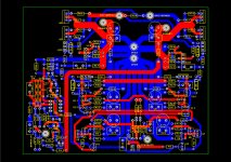
Quick update
Time is a bit limited today. Just posting these as an update. The PCB images are not the best and will be working on a better way to post them. There must be a way without exceeding the image size limits.
Please do not spend too much time trying to read them. The main purpose of this PCB layout is to allow parasitic transfer to simulation. All components on the the schematic suffixed with a B are on the output PCB.
The input PCB will be mounted above the output PCB with the output PCB flat against heatsink. The L//R filter will be remote.
Paul
Attachments
Last edited:
Is this easier to read? Also noticed a track error in the previous version.
I have no 1:1 filing about dimensions but looks like ground tracks can be smaller width. Two sides can be closer in that area and rectangle will be smaller.
- Status
- Not open for further replies.
- Home
- Amplifiers
- Solid State
- Amp design attempt number 2 (simpler)