Member
Joined 2009
Paid Member
Hi OS !
I looked at that link, there are some worrying words "..and is shown, in greatly simpified form..." which means it isn't very simple ?
If I remember, you had a design with Triples which had achieved a similar 'gentle' switching result to the Krill output - where can I find this ?
I looked at that link, there are some worrying words "..and is shown, in greatly simpified form..." which means it isn't very simple ?
If I remember, you had a design with Triples which had achieved a similar 'gentle' switching result to the Krill output - where can I find this ?
Hi OS !
I looked at that link, there are some worrying words "..and is shown, in greatly simpified form..." which means it isn't very simple ?
If I remember, you had a design with Triples which had achieved a similar 'gentle' switching result to the Krill output - where can I find this ?
Yeah , that example just shows a current mirror as a symbol (theory), leaving all the hard work for us crazy hobbyist tinkerers to design a working circuit.
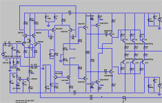
Stuart's implementation is for MOSFETS ,so I can't use his exactly. The spice "guinea pig" , by the way , will be THAT triple (T3T) / symasym amp (attachment 1). The X and Y nodes will attach to a variation of E. Stuart's
(thanks !!! awesome bias page) circuit . The only worry is with the BJT's , I might have to integrate global T comp. into the circuit.
Since I already have the 2 pairs of the working amp , I might be able to go from sim to real quickly.
BTW... LTspice 4.08 (6/23/10) is out. Has more models, more verbose error log , no bugs yet.
OS
Attachments
Last edited:
>I looked at that link, there are some worrying words "
Yes, indeed.
>Stuart's implementation is for MOSFETs
Right. Best results with 2SJ201/2SK1530 (or similar devices).
Cheers,
E.
Yes, indeed.
>Stuart's implementation is for MOSFETs
Right. Best results with 2SJ201/2SK1530 (or similar devices).
Cheers,
E.
Member
Joined 2009
Paid Member
OS, that looks like a darn nice amplifer and with Edmonds bias it will represent state of the art on this forum !
... but the posted schematic uses gnf and what I'm hoping to do is find an output topology I'm happy using without any gnf. Would your triples work without gnf - do they have that Krill soft-turnoff ?
... but the posted schematic uses gnf and what I'm hoping to do is find an output topology I'm happy using without any gnf. Would your triples work without gnf - do they have that Krill soft-turnoff ?
... but the posted schematic uses gnf and what I'm hoping to do is find an output topology I'm happy using without any gnf. Would your triples work without gnf - do they have that Krill soft-turnoff ?
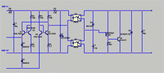
Ahh , GNF !!! The krill , if I remember right , uses GNF .. just not from the OP. instead it takes it from the VAS output. The leach triple takes FB from both the pre - driver stage AND the main OP's , the former the AC component and the latter the DC. Dual feedback paths (Attachment 1) 😀
As far as would the triple work with NO GNF ... of course it would !!
If I took the feedback off the predriver or the VAS , the OP would be out of the loop but there still would be feedback SOMEWHERE. The only drawback to this would be greater THD since the OP would no longer be corrected by GNF.
E Stuarts feedforward scheme might take the place of GNF for the OP .. I will have to complete my Simulations to see.
OS
Attachments
I too like Edmond's approach. I assume there are 3mA CCS attached to X and Y? Very elegant, hats off, Edmond.
I have used nested fb for some time. It is very helpful for stability by reducing OLG and greatly lessens the Zout of the VAS, giving greater control of the output stage.
Hugh
I have used nested fb for some time. It is very helpful for stability by reducing OLG and greatly lessens the Zout of the VAS, giving greater control of the output stage.
Hugh
I assume there are 3mA CCS attached to X and Y?
Hugh
Nope... (attachment 1 ) is what goes on X and Y. First , I will merge the simulation in the attachment to a MOSFET/ IRFP240/9240 version of the above amp (supersym)to determine how this clock ticks. After that , it should be easy to port this to BJT's.
Of course , I will share the sim (file attachment) , too....
OS
Attachments
Last edited:
I too like Edmond's approach. I assume there are 3mA CCS attached to X and Y?
No. Rather a VAS and CCS (or tow complementary VASes).
Very elegant, hats off, Edmond.
Thank you!
Nope... (attachment 1 ) is what goes on X and Y.
Right.
After that , it should be easy to port this to BJT's.
..............
OS
Easy? I'm not sure. Please, notice my remark on BJTs in the article:
'Using bjts instead of mosfets will probably not work at all, as Spice simulations were very discouraging.'
As for the four KSC1845's, no problem during the sim phase. But in real life, please use matched !!! trannies, one THAT300 for example.
Also a 4N28 might give troubles. In the original circuit I've used MCT5211's on purpose, as these opto-couplers have a sufficient high CTR at low LED currents (<1mA).
Cheers,
E.
I will respond to the second statement first. The 1845's are only for simulation .. I would use matched monolithic SMD 2n5550 - http://www.fairchildsemi.com/ds/FF%2FFFB5551.pdf
1-2% match- good for dual.
On to comment 1 , BJT's will require some changes to the circuit. Once I see it's IRF240/9240 simulation , I will rework it. ???? do you have MTC5211 model ?? Here is the mouser page for opto's Transistor Output Optocouplers , what is CTR ?
OS
Member
Joined 2009
Paid Member
Easy? I'm not sure. Please, notice my remark on BJTs in the article:
'Using bjts instead of mosfets will probably not work at all, as Spice simulations were very discouraging.'
This will likely only make OS more determined 😉
I will respond to the second statement first. The 1845's are only for simulation .. I would use matched monolithic SMD 2n5550 - http://www.fairchildsemi.com/ds/FF%2FFFB5551.pdf
1-2% match- good for dual.
Hi OS,
Hmm... Vos isn't specified neither guaranteed. But if smaller than 1 .. 2mV, then it's okay.
On to comment 1 , BJT's will require some changes to the circuit. Once I see it's IRF240/9240 simulation , I will rework it. ???? do you have MTC5211 model ?? Here is the mouser page for opto's Transistor Output Optocouplers , what is CTR ?
OS
CTR means 'Current Transfer Ratio'.
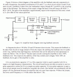
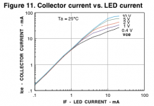
The model I've used is lost, sorry. It was a bit sloppy one. The input was just a AlGaAs IR-LED and the output was a current source, who's output was defined by means of a table, which mimicked the relationship between Id and Ic (see the graph below).
Cheers,
E.
Attachments
Auto Bias Part II
Here it is: Auto Bias part II
Cheers,
E.
Of course I have one! See: Auto Bias
BTW, this design is a bit obsolete. In a few month or so I will update my website with a new version: fully symmetrical and high speed (>1MHz).
Regards,
Edmond.
Here it is: Auto Bias part II
Cheers,
E.
Member
Joined 2009
Paid Member
WOW - this is quite possibly just what I've been looking for. My interest might be to build a zero gain power buffer around this.
When will it be prototyped ?
When will it be prototyped ?
Hello Edmond,
Am I right in thinking that the 3 NPNs need to be matched, and the 3 PNPs need to be matched?
How well matched do the NPNs and PNPs have to be to each other?
Do you have transistor ICs in mind?
Great to see innovative work like this!
Regards,
ihan
Am I right in thinking that the 3 NPNs need to be matched, and the 3 PNPs need to be matched?
How well matched do the NPNs and PNPs have to be to each other?
Do you have transistor ICs in mind?
Great to see innovative work like this!
Regards,
ihan
Last edited:
For example, would a THAT300 & a THAT320 array be suitable?
http://www.thatcorp.com/datashts/THAT_300-Series_Datasheet.pdf
http://www.thatcorp.com/datashts/THAT_300-Series_Datasheet.pdf
"Autobias and Error Correction for MOSFET and BJT Audio Output Stages"
It will do BJT's ,too. 😎 I will throw this into the "mongrel" . It looks a bit simpler , as well.
Any fast bipolar , well matched... will do ??
how would one integrate T comp into this circuit ?
Or is it already there? (Q1-2 ?)
OS
It will do BJT's ,too. 😎 I will throw this into the "mongrel" . It looks a bit simpler , as well.
Any fast bipolar , well matched... will do ??
how would one integrate T comp into this circuit ?
Or is it already there? (Q1-2 ?)
OS
Last edited:
Hi all,
>prototyped?
Probably never. I'm a designer rather than a builder.
Yes. All NPNs to NPNs, respectively all PNPs to PNPs.
Not that precise, see next next answer.
Yes I do. For the NPNs a THAT300 and for the PNPs a THAT320.
Thanks!
That's right. Preferable Vos (i.e. delta Vbe) should be smaller than 1mV.
Also the CCSs should be matched, say within a few percent.
I would say, just simulate the thing, add an off-set voltage to one (or more) of the bases of Q1...Q6 and/or the trannies of constant current sources, and see what happens. The bias voltage between the gates or bases of the OPS should under no circumstances collapse.
Yes, it's already there. It's not only Q1/2 that does the temp. comp., instead it's the bias circuit as a whole that provides the temp. compensation of drivers and output transistor.
But the autobias circuit itself does have a temp. coefficient, though far less than most of the common output stages, i.e. 0.3% / K. Please see also the 'math' on my website.
At room temperature of the bias circuit (and independently of the OPS temp.), the voltage across the emitter/source resistors is fixed at VT. ln 3 = 28.5mV. IOW, Iq of the OPS does not vary with temperature of the O/P devices, but only with the temperature of Q1...Q6 (the THATxxx chips).
(VT is the so called 'thermal voltage', about 26mV at room temp.)
Cheers,
E.
edit: In case of BJTs in the OPS, I would recommend a triplet topology.
WOW - this is quite possibly just what I've been looking for. My interest might be to build a zero gain power buffer around this.
When will it be prototyped ?
>prototyped?
Probably never. I'm a designer rather than a builder.
Hello Edmond,
Am I right in thinking that the 3 NPNs need to be matched, and the 3 PNPs need to be matched?
Yes. All NPNs to NPNs, respectively all PNPs to PNPs.
How well matched do the NPNs and PNPs have to be to each other?
Not that precise, see next next answer.
Do you have transistor ICs in mind?
Yes I do. For the NPNs a THAT300 and for the PNPs a THAT320.
Great to see innovative work like this!
Regards,
ihan
Thanks!
For example, would a THAT300 & a THAT320 array be suitable?
Yes indeed, these are suitable candidates.
http://www.thatcorp.com/datashts/THAT_300-Series_Datasheet.pdf
"Autobias and Error Correction for MOSFET and BJT Audio Output Stages"
It will do BJT's ,too. 😎 I will throw this into the "mongrel" . It looks a bit simpler , as well.
Any fast bipolar , well matched... will do ??
That's right. Preferable Vos (i.e. delta Vbe) should be smaller than 1mV.
Also the CCSs should be matched, say within a few percent.
I would say, just simulate the thing, add an off-set voltage to one (or more) of the bases of Q1...Q6 and/or the trannies of constant current sources, and see what happens. The bias voltage between the gates or bases of the OPS should under no circumstances collapse.
how would one integrate T comp into this circuit ?
Or is it already there? (Q1-2 ?)
OS
Yes, it's already there. It's not only Q1/2 that does the temp. comp., instead it's the bias circuit as a whole that provides the temp. compensation of drivers and output transistor.
But the autobias circuit itself does have a temp. coefficient, though far less than most of the common output stages, i.e. 0.3% / K. Please see also the 'math' on my website.
At room temperature of the bias circuit (and independently of the OPS temp.), the voltage across the emitter/source resistors is fixed at VT. ln 3 = 28.5mV. IOW, Iq of the OPS does not vary with temperature of the O/P devices, but only with the temperature of Q1...Q6 (the THATxxx chips).
(VT is the so called 'thermal voltage', about 26mV at room temp.)
Cheers,
E.
edit: In case of BJTs in the OPS, I would recommend a triplet topology.
Last edited:
Member
Joined 2009
Paid Member
Edmond, the harmonic distortion profile looks very 'Hiraga' like. Which I consider good. But I'm not sure I have understood the vertical scale on the plot - it looks like distortion products at several % points, which is not good ?
several % points ?
Hi Bigun,
Apparently you don't know me very well yet 😉
I would never publish an OPS with so much distortion.
Anyhow, the scale is in milli % and the THD about 0.01%.
As for a'Hiraga like' spectrum, indeed it looks nice. But remember, this is the spectrum of the OPS in isolation. If implemented in a complete amp with global NFB and Miller compensation, the global loop gain will show a roll-off by 6dB/octave. As a result, you will get a different picture: Although much lower, the spectrum will be CCW 'tilted' by 6dB/octave.
Cheers,
E.
PS: To avoid the confusion I've updated the website. Thx!
- Status
- Not open for further replies.
- Home
- Amplifiers
- Solid State
- Variable operating biass output ?