Congratulations Edmond ! Your latest contraption looks like a genuine advance in class AB design.
Hi Vladn,
Thank you for kind words.
Definitely worth a publication
Perhaps in EDN.
and perhaps a patent application (if you want to commercialize the idea).
In Europe, a patent is ridiculous expensive, far far more than in the US. So little chance to earn back the investment.

Therefore, I place my ideas in the public domain. Then it is 'prior art' and no one else can apply for a patent any longer, provided, of course, that the patent authorities do their homework well enough.
Works nice in simulation even with switching mosfets (although due to high threshold these would benefit from bootstrap powered CCSs/drivers to get full rail output).
Indeed, it works with any output device. As for bootstrapping, sure you can do that if you want to squeeze out the last volts. On the other hand, in particular with high NFB designs, under such conditions, the sky rocketing Cgd will cause severe instability issues.
Anyhow, I will also look at possible and practical bootstrapped configurations. Perhaps the 'old skool' RC networks will do.
Cheers,
E.
I've tried using shared bootstrap with plain resistors instead of CCSes connected to it and it works OK too. THD is higher, mainly due to voltage gain loss in the first (allison-like) stage. But stability w.r.t. PS voltage variation is not too bad and it may be usable in such configuration.Perhaps the 'old skool' RC networks will do.
Also tried separate bootstraps - front pair load Rs bootstrapped from the gate buffers (separately), sensing quad load Rs bootstrapped from the output. Much better THD relative to the common bootstrap, not quite as good as original CCSes (at low frequencies) but still very nice.
One thing that needs some attention is clipping behavior and square wave response. Some strategically placed anti-saturation clamps may be needed to get reasonably clean output when control loop envelope is exceeded. Separate signal paths for upper/lower output devices is a downside of nearly all EC/fast bias control schemes, it is harder to get nice impulse response with high slew rate demand.
One thing that needs some attention is clipping behavior and square wave response. Some strategically placed anti-saturation clamps may be needed to get reasonably clean output when control loop envelope is exceeded. Separate signal paths for upper/lower output devices is a downside of nearly all EC/fast bias control schemes, it is harder to get nice impulse response with high slew rate demand.
Also tried separate bootstraps - front pair load Rs bootstrapped from the gate buffers (separately), sensing quad load Rs bootstrapped from the output. Much better THD relative to the common bootstrap, not quite as good as original CCSes (at low frequencies) but still very nice.
Hi Vladn,
Thanks for figuring this out. Somewhat higher distortion at LF is quite predictable, as the loop gain is lowered by the resistors. Not a serious problem, I think.
One thing that needs some attention is clipping behavior and square wave response. Some strategically placed anti-saturation clamps may be needed to get reasonably clean output when control loop envelope is exceeded.
That's right. Did you notice my remark on this topic?
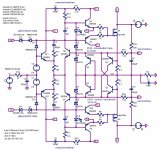
Anyway, here's an example of where to put the clamps: AB-OPS10
BTW, this is NOT the schematic of my final version.
Separate signal paths for upper/lower output devices is a downside of nearly all EC/fast bias control schemes, it is harder to get nice impulse response with high slew rate demand.
Hmm... I was quite happy with the step response. Also very fast: about 1.5GV/s.
See: Auto Bias part II Fig. 5
Perhaps it has something to do with a higher Vgs in your version.
Could you drop a picture of your results, so we can compare them?
Cheers,
E.
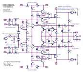
Tried compounded bootstrap for the front EC transistor pair load - this one works almost as good as CCSes even at low frequencies but with the full rail to rail output using cheap high threshold switching mosfets ! Attached is the schematics based on Edmond's ideas with the bootstraps instead of CCSes. (selection of transistors is for general testing only)
Also found the main culprit of weird square wave response - it was non-linear interaction between my gate protection clamps and compensation/forwarding capacitors. Added "forwarding" diodes (Edmond's AB-OPS10 schematics D3,D4, my schematics D11,D12) and now both high slew rate square wave response and clipping look clean ! Also added diodes for reverse Vcb protection on the sensing pair.
Also found the main culprit of weird square wave response - it was non-linear interaction between my gate protection clamps and compensation/forwarding capacitors. Added "forwarding" diodes (Edmond's AB-OPS10 schematics D3,D4, my schematics D11,D12) and now both high slew rate square wave response and clipping look clean ! Also added diodes for reverse Vcb protection on the sensing pair.
Attachments
Last edited:
Member
Joined 2009
Paid Member
I like it - I like Bootstrapping in general, seems to offer some advantages in terms of sound quality in certain topologies, is cost effective and reliable.
Tried compounded bootstrap for the front EC transistor pair load - this one works almost as good as CCSes even at low frequencies but with the full rail to rail output using cheap high threshold switching mosfets !
[snip]
Hi Vladn,
Good work! Thanks for your input.
To all,
Notice the frequency compensation. To a certain extent it also acts as a feed forward compensation, in the same way as in Bob's EC amp. See: Cordell Audio: Papers: A MOSFET Power Amplifier with Error Correction , R36 & C6, respectively R37 & C7.
As such compensation schemes simply bypass the EC circuitry at HF, the funny thing is that the amp still works if the comp. caps are increased even by a factor of thousand (of course at the expense of increased distortion).
BTW, you can't do this with a LT1166, which relies on shunt compensation. See the data sheet, Fig.3, Cext1 & Cext2. (bad practice!)
Cheers,
E.
Few more notes on bootstraps:
1. By adding a constant voltage drop (zener or LEDs valued close to the mosfet treshold voltage) in series with R15,R16 (on my schematics) it is possible to achieve near zero (or even negative) dependence of Iq and Imin on VCC. (obviously R15,R16 should be correspondingly adjusted)
2. With high threshold mosfets and bootstrap it probably makes sense to power Q7,Q10 collectors from the output node, this way collectors of both driver transistors are bootstrapped for AC and their miller capacitances neutralized.
3. Paradoxically, common mode PSRR is slightly (about 6db) BETTER with the bootstrap compared to CCSes. Perhaps I have made a mistake somewhere in my simulation, perhaps it is due to bootstrapped gate driver power.
Some yet unexplained things from my simulation:
1. There is an optimum VAS impedance (around 1.5k) that yields noticeably lower distortion at low frequencies, the distortion is lower than if you simply bypass the first follower pair with a low impedance source; it is either intrinsic error compensation effect or simulation fluke, I do not know yet.
2. Attempt to drive the front follower collectors directly from bootstrap rather than driver output slightly increased THD even though using bootstrap voltage for the follower should be slightly cleaner for several reasons.
Mind you, I am talking 1kHz THDs on the order of 0.0002% and 100Hz THD below 0.0001% from the output stage alone on a 4ohm load so these could be either sim artifacts or stupid me doing something wrong.
Few more notes on bootstraps:
1. By adding a constant voltage drop (zener or LEDs valued close to the mosfet treshold voltage) in series with R15,R16 (on my schematics) it is possible to achieve near zero (or even negative) dependence of Iq and Imin on VCC. (obviously R15,R16 should be correspondingly adjusted)
Clever!
2. With high threshold mosfets and bootstrap it probably makes sense to power Q7,Q10 collectors from the output node, this way collectors of both driver transistors are bootstrapped for AC and their miller capacitances neutralized.
Surely, you can do that, but make sure there is still sufficient headroom for Q7 and Q10 when subjected to large and fast transients.
3. Paradoxically, common mode PSRR is slightly (about 6db) BETTER with the bootstrap compared to CCSes. Perhaps I have made a mistake somewhere in my simulation, perhaps it is due to bootstrapped gate driver power.
Some yet unexplained things from my simulation:
1. There is an optimum VAS impedance (around 1.5k) that yields noticeably lower distortion at low frequencies, the distortion is lower than if you simply bypass the first follower pair with a low impedance source; it is either intrinsic error compensation effect or simulation fluke, I do not know yet.
2. Attempt to drive the front follower collectors directly from bootstrap rather than driver output slightly increased THD even though using bootstrap voltage for the follower should be slightly cleaner for several reasons.
Mind you, I am talking 1kHz THDs on the order of 0.0002% and 100Hz THD below 0.0001% from the output stage alone on a 4ohm load so these could be either sim artifacts or stupid me doing something wrong.
May times I've observed similar paradoxical effects. Most likely two or more antagonistic distortion mechanisms are involved.
Cheers,
E.
I understand, but how much headroom the bias circuit allows in that direction ? Take your V4 sensor configuration - the excursion is limited by intrinsic collector-base diode of the sensor transistor so it can go no further than opposite Rd (mosfet drain resistor) potential + one Vcb. Unless I miss something (quite possible) it makes sense to tie driver collectors to the opposite Rd instead of the output node. Perhaps a clamp is needed to prevent sensor transistor collector-base diode from conducting and driver transistor from saturating. On my diagram this is handled by D6,D7 but the excursion is limited by output node plus voltage across two schottky diodes. I may try to re-arrange things a bit.Surely, you can do that, but make sure there is still sufficient headroom for Q7 and Q10 when subjected to large and fast transients.
Last edited:
Things are a bit complicated with driver swing in the mosfet turn-off direction. First your V4 topology limits that range with last pair collector diodes. OK, this can be easily fixed by adding schottky diodes in series with sensor pair collectors (V4 topology of the final pair). Next problem is reverse Vbe breakdown on entire sensing quad. That is why it is unfortunately unsafe to clamp the the sensor quad emitters to the opposite Rd - momentary current excursions could easily exceed Vbe breakdown. Mosfet gate clamp is too far away.
And yet it is true that transient response is noticeably worse with a simple clamp to the output node (like on my diagram) compared to no clamp (especially with series schottky diodes in V4 last sensor pair collectors).
The only clean option to allow a bit of extra room (as I see it) is another zener clamp (few volts) from the sensor emitters to the output node safe for reverse Vbe, plus series schottky in the collectors of the final pair. Where to tie driver collectors depends on how this clamping is defined.
A radical solution is to somehow completely bypass EC stage once it goes into saturation (clipping, transients). But it is not trivial, need to think about it.
I understand, but how much headroom the bias circuit allows in that direction ? Take your V4 sensor configuration - the excursion is limited by intrinsic collector-base diode of the sensor transistor so it can go no further than opposite Rd (mosfet drain resistor) potential + one Vcb. Unless I miss something (quite possible) it makes sense to tie driver collectors to the opposite Rd instead of the output node.
No, you didn't miss anything, rather I was confusing a few things. I once tied those collectors to the output (and observed troubles) but that was an OPS without auto bias circuitry and with MOSFETs with a much lower Vgsth.
So you are right. In this case the headroom is already limited by the auto bias stuff.
Perhaps a clamp is needed to prevent sensor transistor collector-base diode from conducting and driver transistor from saturating. On my diagram this is handled by D6,D7 but the excursion is limited by output node plus voltage across two schottky diodes. I may try to re-arrange things a bit.
Yes, a clamp to be on the safe side. But what about a LP filter at the very input, preferable a 2nd order filter, in oder to keep out fast transients? Besides, this also will releases the maximum stress on the drivers.
Cheers,
E.
(PS, I have to leave now.Till tomorrow)
Just to illustrate brute force / safe approach I am attaching v2 of my diagram. I am sure things could be done more elegantly. Note that I ended up connecting front follower collectors to the bootstrap directly, despite slightly higher THD (puzzling) the impulse response is noticeably cleaner this way.
Regarding LP in the front - no doubt about it, but for an amp in this class it is nice to have an output stage do >1GV/s cleanly 🙂
Regarding LP in the front - no doubt about it, but for an amp in this class it is nice to have an output stage do >1GV/s cleanly 🙂
Attachments

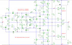
equalizing the currents
And here is a 'hybrid' solution. No split bootstrapped circuits, instead two additional trannies (Q13 resp. Q14) that simply copy the current through the bias generator (Q11 resp. Q12) of the push-pull drivers. This way it's guaranteed that all currents fed to the auto bias circuit are identical and don't depend on Vgs.
Nevertheless, I wouldn't recommend this solution, as the distortion, compared to the original circuit, is considerably higher.
Apparently, you can't have them all: auto bias,maximum output swing, low distortion and 1GV/s slew rate.
Cheers,
E.
PS: Maybe this circuit needs more protection stuff, but at the moment, I'm not in the mood to figure that all out. Sorry.
Attachments

That is precisely why I ended up using compound bootstrap as a load for the front EC transistor pair ! It works almost indistinguishable from the CCS version both for THD and dynamics.Nevertheless, I wouldn't recommend this solution, as the distortion, compared to the original circuit, is considerably higher.
At any rate your idea is both clever and unique. It caught my attention immediately and I had a blast playing with it in the sim and learning the subtleties of it's operation. I hope I did not hijacked the thread or otherwise caused any distraction of any kind with my overenthusiastic response 🙂.
P.S. I ended up connecting protection diodes D17,D20 (on my last diagram) to the mosfet drains instead of the output node. This way the worst case scenario of Vbe reversal on sense transistors is handled correctly (I think).
That is precisely why I ended up using compound bootstrap as a load for the front EC transistor pair ! It works almost indistinguishable from the CCS version both for THD and dynamics.
My sim results weren't that bad when using single/common bootstraps. The only thing I did wrong was the current equalizing stuff. Now it's much better. Same components, but connected in a slightly different way: see below, Q9, Q12, R14 & R15. Now the current sources for the sens trannies are 'automatically' adjusted for any Vgs.
Compared to the CCS version, THD-20k is (only) 10% higher.
At any rate your idea is both clever and unique.
Thank you!
It caught my attention immediately and I had a blast playing with it in the sim and learning the subtleties of it's operation.
Happily, you are one of the few who see the potential of this circuit.
I wonder how many more people recognize it. Perhaps Mr Krill? 🙄
I hope I did not hijacked the thread or otherwise caused any distraction of any kind with my overenthusiastic response 🙂.
Don't worry. Quite the opposite. I'm glad you jumped on this subject and provided some improvements and/or additions.
P.S. I ended up connecting protection diodes D17,D20 (on my last diagram) to the mosfet drains instead of the output node. This way the worst case scenario of Vbe reversal on sense transistors is handled correctly (I think).
Thanks. As you see, I've also incorporated them in my latest version.
If you think this circuit needs more or other protection stuff, please let me know.
BTW, do you have THATxxx models? Otherwise, I can send them to you.
Cheers,
E.
PS: Q13 & Q15, respectively Q14 & Q18, should be thermally coupled.
Attachments
Sure, why not, the more models the better 🙂. However I think the main source of simulation accuracy error is really the mosfet model. Your circuit happily avoids the worst modeled Gm region but I have little confidence in Cgd accuracy. Less of an issue for your laterals though.BTW, do you have THATxxx models? Otherwise, I can send them to you.
I went through several bootstrap configurations, recovering THD difference at successfully lower frequencies. Points C,D (on your schematics) are relatively low impedance (about 13ohm at 1ma per pair) and their CC load AC impedance is not very critical. However points A,B require very high impedance from the CS bootstrap if you want high error correction gain and the mosfet gate voltage does not follow the output node, hence I came up with the compound bootstrap idea. If/when you have time/desire - try it out, just split R16,R21 and add a cap from outer driver emitters to the midpoints. It pretty much closes the THD gap at low frequencies.My sim results weren't that bad when using single/common bootstraps.
PS I think D9/D10 are redundant on your last schematics because of D5-D8.
Last edited:
Sure, why not, the more models the better 🙂. However I think the main source of simulation accuracy error is really the mosfet model. Your circuit happily avoids the worst modeled Gm region but I have little confidence in Cgd accuracy. Less of an issue for your laterals though.
Yes, I know Cgd isn't accurately modeled. Currently, I'm using two models: one for maximum simulation speed, which is simply based on a diode, and one for accuracy based on tanh functions (courtesy of Andy_C). But the latter burns many CPU cycles.
I don't think accuracy is that important as long as the models comply with the worst case conditions (i.e. min. and max. Cgd)
I went through several bootstrap configurations, recovering THD difference at successfully lower frequencies. Points C,D (on your schematics) are relatively low impedance (about 13ohm at 1ma per pair) and their CC load AC impedance is not very critical. However points A,B require very high impedance from the CS bootstrap if you want high error correction gain and the mosfet gate voltage does not follow the output node, hence I came up with the compound bootstrap idea. If/when you have time/desire - try it out, just split R16,R21 and add a cap from outer driver emitters to the midpoints. It pretty much closes the THD gap at low frequencies.
I've tried that too, results are probably more or less in accordance with yours.
These are my THD figures at 20Hz:
Using const. current sources:THD20Hz = 8.4ppb
Using common bootstraps: THD20Hz = 2.5ppb
Using separate bootstraps: THD20Hz = 0.7ppb
With a real life front-end, above figures will be of course higher (and most likely identical in all three cases, as the distortion of the IPS and/or VAS will dominate).
But shouldn't we look at the worst case conditions, that is, at 20kHz? Then the differences are much smaller:
const. current sources:THD20kHz = 4.96ppm
common bootstraps: THD20kHz = 6.16ppm
separate bootstraps: THD20kHz = 5.65ppm
PS I think D9/D10 are redundant on your last schematics because of D5-D8.
They certainly look redundant, but without them the peak currents through D5 and D6 exceeded the max. rating. OTOH, maybe it wasn't a realistic test, so they aren't needed in real life. Together with a low pass filter in front of the input (to keep out HF interference) peak currents are much lower anyhow.
Cheers,
E.
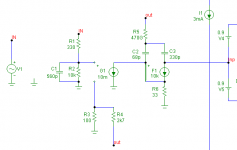
Below the front-end used for the sims. ULGF = 1MHz. R5 = 470G -> ordinary Miller compensation. R5 = 470R -> TMC.
Attachments
- Status
- Not open for further replies.
- Home
- Amplifiers
- Solid State
- Variable operating biass output ?