Hi Edmond, welcome back !
About the OPS I have MJ15003/4 pairs ans 2SJ162/SK1058 pairs. I would prefere going for the LATERAL MOSFET 2SJ162/SK1058 ... I would go up to 4 pairs per channel.
I would like to drive 250 or more W into 8 ohms and also be able without issue to drive 4 ohms too at full power.
Initially i would go for a raw DC rectified PSU with around 75 to 85 V depending on the needs
I read it can be wise to have one regulated supply too for the IS and VA stage ... is that right?
Take your time to analyse but i think the CMCL included now seems to work fine.
But I do not really see how it works ... could you give some word of explanation ...?
Till later
Schol
Olivier
Edmond, while you check the circuit (which i send you here in .cir format)...
What do you think is necessary to incorporate next in the VAS and IS? Not yet the OPS ...
I think of :
other protection stuff, like the diodes you placed in the IS (clamp?)
Self places 4 diodes accros the feedback cap whereas Slone places only 1 like it is in the schematic now. Whats best?
You placed some other capacitors in the IS and just before the input of the VAS ... ould these be incorporated? Maybe just routed on the pcb in case?
Do you think it is wise to cascode the input stage?
Self also talks about radical methods in the IS ... Cascomp(?) , Quad something, ...
Another thing :
In the 2SA1381 Q the SOA spec specifies a TA graph and a TC graph. The TA one is very difficult to attein as it limits the values very hardly ... The TC line is better ...
What is that difference?
TA = without heatsink or what?
Hope to read you soon
Bye
Olivier
Attachments
Cmcl
Hi Olivier,
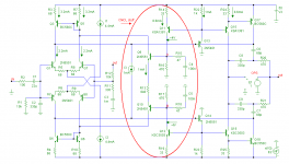
Okay, let's try to explain that CMCL thingy. Below you see a simplified circuit with only the main components of a CMCL (and TMC of course 😉). Our aim is to stabilize the standing VAS current in a well controlled manner. This means that sum of the (absolute value of) top and bottom VAS should be held at a constant value. As we have no direct access to these currents, we are using a copy of them (see Q11 & Q12) and look at the collector currents of these copies instead.
Each of these (copied) currents creates a voltage drop across R16 respectively R17. Now the sum of these voltages (i.e. the voltage between A and B) is proportional to the sum of the VAS currents: V(A,B) = (|Ic(Q11)| + Ic(Q12) ) * 470
This sum in turn is sensed by Q9, Q10, R13 and converted to a current Is.
Is = ( ( |Ic(Q11)| + Ic(Q12) ) * 470 - 2*Vbe ) / 6k8
The higher the VAS currents, the higher Is.
Is is subtracted from the VAS inputs via the current mirrors. But without a constant reference current, which is added to the VAS inputs, it shouldn't work as the VASes are completely turned off. Therefore I've added a reference current I3 = 1mA. So Is is compared against I3.
Is = ( ( |Ic(Q11)| + Ic(Q12) ) * 470 - 2*Vbe ) / 6k8 = 1mA
( |Ic(Q11)| + Ic(Q12) ) * 470 - 2*Vbe = 6.8
( |Ic(Q11)| + Ic(Q12) ) * 470 ~= 8
|Ic(Q11)| + Ic(Q12) ~= 8/470 = 17mA
|Ic(Q11)| = Ic(Q12) ~= 8.5mA
Simple, isn't it?
Gegroet, Edmond.
BTW, C4, C5, R15 & R18 define the unity loop gain frequency and phase of the CMCL. ULGF = 500kHz and the phase margin = 90 degrees.
The DC loop gain is quite high, about 47dB, so disturbances from imbalance etc. are highly suppressed.
Hi Edmond, welcome back !
[snip]
But I do not really see how it works ... could you give some word of explanation ...?
Till later
Schol
Olivier
Hi Olivier,
Okay, let's try to explain that CMCL thingy. Below you see a simplified circuit with only the main components of a CMCL (and TMC of course 😉). Our aim is to stabilize the standing VAS current in a well controlled manner. This means that sum of the (absolute value of) top and bottom VAS should be held at a constant value. As we have no direct access to these currents, we are using a copy of them (see Q11 & Q12) and look at the collector currents of these copies instead.
Each of these (copied) currents creates a voltage drop across R16 respectively R17. Now the sum of these voltages (i.e. the voltage between A and B) is proportional to the sum of the VAS currents: V(A,B) = (|Ic(Q11)| + Ic(Q12) ) * 470
This sum in turn is sensed by Q9, Q10, R13 and converted to a current Is.
Is = ( ( |Ic(Q11)| + Ic(Q12) ) * 470 - 2*Vbe ) / 6k8
The higher the VAS currents, the higher Is.
Is is subtracted from the VAS inputs via the current mirrors. But without a constant reference current, which is added to the VAS inputs, it shouldn't work as the VASes are completely turned off. Therefore I've added a reference current I3 = 1mA. So Is is compared against I3.
Is = ( ( |Ic(Q11)| + Ic(Q12) ) * 470 - 2*Vbe ) / 6k8 = 1mA
( |Ic(Q11)| + Ic(Q12) ) * 470 - 2*Vbe = 6.8
( |Ic(Q11)| + Ic(Q12) ) * 470 ~= 8
|Ic(Q11)| + Ic(Q12) ~= 8/470 = 17mA
|Ic(Q11)| = Ic(Q12) ~= 8.5mA
Simple, isn't it?
Gegroet, Edmond.
BTW, C4, C5, R15 & R18 define the unity loop gain frequency and phase of the CMCL. ULGF = 500kHz and the phase margin = 90 degrees.
The DC loop gain is quite high, about 47dB, so disturbances from imbalance etc. are highly suppressed.
Attachments
Edmond, while you check the circuit (which i send you here in .cir format)...
What do you think is necessary to incorporate next in the VAS and IS? Not yet the OPS ...
I think of :
other protection stuff, like the diodes you placed in the IS (clamp?)
Hi Olivier,
I would certainly recommend a clamp, see one my previous schematics, 8 diodes + 3 resistor.
Self places 4 diodes across the feedback cap whereas Slone places only 1 like it is in the schematic now. Whats best?
Self's solution is slightly better (at LF).
You placed some other capacitors in the IS and just before the input of the VAS ... should these be incorporated? Maybe just routed on the pcb in case?
These caps and Rs are not always necessary, but it's wise to route them on the PCB anyway. Better safe then sorry.
Anyhow, check the phase margin of the Miller loop by means of Middlebrook's method.
See: Simulating Loop Gain - Spring 1997
Do you think it is wise to cascode the input stage?
Self also talks about radical methods in the IS ... Cascomp(?) , Quad something, ...
Not really necessary, though it depends on the maximum distortion you are willing to accept.
Another thing :
In the 2SA1381 Q the SOA spec specifies a TA graph and a TC graph. The TA one is very difficult to attein as it limits the values very hardly ... The TC line is better ...
What is that difference?
TA = without heatsink or what?
TA = ambient temperature = without heat sink.
TC = case temperature = with (large) heat sink.
If the SOA is exceeded, try a lower Ic. As for the VAS, this is no problem if the drivers take care of sufficient current gain. In case of MOSFET output devices one pair of drivers is okay. In case of BJT output devices, use an additional pre-driver (i.e. a triplet OPS).
Hope to read you soon
Bye
Olivier
Cheers,
Edmond.
long question for Edmond
🙂 hi Edmond,
I was in your country today at Arnhem... stopped to have a burger king on the way ! We don't have them in Belgium just Mc & Quick ;-)
About the project :
Since I will most probably use a MOSFET. Lets say 4 pairs per channel, I will just use one driver stage between the VAS and OPS. Is that still OK? I understood MOSFETS are voltage devices which draw only small amount of currrent even while operating at capacity (no beta droop). But is 4 combined still OK?
I will insert the clamp diodes in the circuit as in your design however for now I limit the schematic the IS and VAS. Before I go further I will construct that IS & VAS and test it deeply (even lab THD+N, I think I can test it in a professional measurement lab. Not sure yet). It might be a waste of money but I will design a PCB just for that even if I need to redesign one adding the OPS later. But I want to exclude OPS related and even OPS PCB related issues, in order to isolate IS & VAS issues solely.
So for clamps it's just the IS clamps right?
In my next posting I will send the latest .CIR schematic. Incorporating IS clamps, 4-diode system around the feedback Capacitor and additional resistor and cap filters in the IS & VAS.
I changed the load resistance to 20 kOhms.
I used once the input conditionning circuit of Slone, which is a second order circuit. It contains a series resistor of around 5K which reduces the CLG with 3dB over the whole bandwidth due to a voltage dividing with Zin of the amp I suppose. It greatly reduces the HF roll-off point wich is rather good because it happens second order, -40dB/decade. What I find more strange is that it raises the THD at 1KHz full load to about 10x the value compared to the schematic with this input circuit. This resistor is only a linear division no? Why does it distort then?😕
However I write this before the clamps are introduced the THD at 1kHz is less than 5u% 😀😀😀 However load is raised to 20K as stated above and output Vpp is now 106V for a summed rail potental of 126V. Going higher in the output raises THD considerably. I will see later if it is worth sacrificing THD for output swing but I think it will since it is useless to have low THD while output power is near zero 🙄
To reach the optimum THD the Iq VAS is around 26mA. I find that acceptable even if for the Q's it is a bit on the high side, I will certainly heatsink them anyway. If necessary I can still reduce to 20mA or 15mA but going lower is not good I believe. What do you think?
The is another weird finding. When testing for THD I noticed it rises quite steeply with increasing frequency. According to Slone, the THD figure at 20kHz should be nearly 10x higher than at 1 kHz. First of all is that reasonable? Hereunder my simulation results, however I needed to fiddle with the time step because with higher frequency and equal time step the simulation FFT shows funny signs like adding 100u% at some higher harmonics 10th for instance ... nothing on harmonic 6, 7, 8, 9, then a lot at the 10th and none at the 11th but then again 100u% at the 12th harmonic... weird isn't it? However if that happened I reduced timestep e.g. from 0.05u to 0.01u and the problem went away ... so here the results :
01KHz : 4.4u%
05KHz : 18u%
10KHz : 105u%
15KHz : 340u%
20KHz : 800u%
50KHz : 1300u% ( 13m% or 0.013% )
You see? @ 20kHz the THD is nearly 200 times higher ! Slone says 10x 😱😱😱 I could accept 15x or even 20x but nearly 200x ??? Do you see where this could come from? What is the cause of this? Differential imbalance? Current starvation? TMC? Or do I measure wrong?
I tried raising I-tail => no chane (or weak)
I removed TMC to simple miller cap => no change at all
BUT BUT BUT Edmond 😀😀😀 great sinner as I am I tried the old TPC again and guess what !
01KHz : 3.3u%
20KHz : 7u%
50KHz : 50u%
This drawing follows closely Slones Prediction, the 10x THD occurs at around 25KHz instead of 20KHz but that is normal because its just a ballparc approximation ... I guess this is because at high frequencys, well seeable with a squarewave signal, a TPC generates an overshoot, this is bad but it is faster and can keep up the pace wheras a single miller cap or TMC dont allow overshoot causing a too much damped rise and eventually never getting to the top before the signal needs to go down again.
But hey, the overshoot can surely be a nasty thing too 😛
Some other question :
Off topic since I dont go into OPSs yet...
Using MOSFETS should I use a source follower or a complementary feedback? What type of protection to use?
OK enough blabla for now 🙄 I implement the latest things and send it up...
Groeten,
Olivier
🙂 hi Edmond,
I was in your country today at Arnhem... stopped to have a burger king on the way ! We don't have them in Belgium just Mc & Quick ;-)
About the project :
Since I will most probably use a MOSFET. Lets say 4 pairs per channel, I will just use one driver stage between the VAS and OPS. Is that still OK? I understood MOSFETS are voltage devices which draw only small amount of currrent even while operating at capacity (no beta droop). But is 4 combined still OK?
I will insert the clamp diodes in the circuit as in your design however for now I limit the schematic the IS and VAS. Before I go further I will construct that IS & VAS and test it deeply (even lab THD+N, I think I can test it in a professional measurement lab. Not sure yet). It might be a waste of money but I will design a PCB just for that even if I need to redesign one adding the OPS later. But I want to exclude OPS related and even OPS PCB related issues, in order to isolate IS & VAS issues solely.
So for clamps it's just the IS clamps right?
In my next posting I will send the latest .CIR schematic. Incorporating IS clamps, 4-diode system around the feedback Capacitor and additional resistor and cap filters in the IS & VAS.
I changed the load resistance to 20 kOhms.
I used once the input conditionning circuit of Slone, which is a second order circuit. It contains a series resistor of around 5K which reduces the CLG with 3dB over the whole bandwidth due to a voltage dividing with Zin of the amp I suppose. It greatly reduces the HF roll-off point wich is rather good because it happens second order, -40dB/decade. What I find more strange is that it raises the THD at 1KHz full load to about 10x the value compared to the schematic with this input circuit. This resistor is only a linear division no? Why does it distort then?😕
However I write this before the clamps are introduced the THD at 1kHz is less than 5u% 😀😀😀 However load is raised to 20K as stated above and output Vpp is now 106V for a summed rail potental of 126V. Going higher in the output raises THD considerably. I will see later if it is worth sacrificing THD for output swing but I think it will since it is useless to have low THD while output power is near zero 🙄
To reach the optimum THD the Iq VAS is around 26mA. I find that acceptable even if for the Q's it is a bit on the high side, I will certainly heatsink them anyway. If necessary I can still reduce to 20mA or 15mA but going lower is not good I believe. What do you think?
The is another weird finding. When testing for THD I noticed it rises quite steeply with increasing frequency. According to Slone, the THD figure at 20kHz should be nearly 10x higher than at 1 kHz. First of all is that reasonable? Hereunder my simulation results, however I needed to fiddle with the time step because with higher frequency and equal time step the simulation FFT shows funny signs like adding 100u% at some higher harmonics 10th for instance ... nothing on harmonic 6, 7, 8, 9, then a lot at the 10th and none at the 11th but then again 100u% at the 12th harmonic... weird isn't it? However if that happened I reduced timestep e.g. from 0.05u to 0.01u and the problem went away ... so here the results :
01KHz : 4.4u%
05KHz : 18u%
10KHz : 105u%
15KHz : 340u%
20KHz : 800u%
50KHz : 1300u% ( 13m% or 0.013% )
You see? @ 20kHz the THD is nearly 200 times higher ! Slone says 10x 😱😱😱 I could accept 15x or even 20x but nearly 200x ??? Do you see where this could come from? What is the cause of this? Differential imbalance? Current starvation? TMC? Or do I measure wrong?
I tried raising I-tail => no chane (or weak)
I removed TMC to simple miller cap => no change at all
BUT BUT BUT Edmond 😀😀😀 great sinner as I am I tried the old TPC
again and guess what ! 01KHz : 3.3u%
20KHz : 7u%
50KHz : 50u%
This drawing follows closely Slones Prediction, the 10x THD occurs at around 25KHz instead of 20KHz but that is normal because its just a ballparc approximation ... I guess this is because at high frequencys, well seeable with a squarewave signal, a TPC generates an overshoot, this is bad but it is faster and can keep up the pace wheras a single miller cap or TMC dont allow overshoot causing a too much damped rise and eventually never getting to the top before the signal needs to go down again.
But hey, the overshoot can surely be a nasty thing too 😛
Some other question :
Off topic since I dont go into OPSs yet...
Using MOSFETS should I use a source follower or a complementary feedback? What type of protection to use?
OK enough blabla for now 🙄 I implement the latest things and send it up...
Groeten,
Olivier
🙂 hi Edmond,
I was in your country today at Arnhem... stopped to have a burger king on the way ! We don't have them in Belgium just Mc & Quick ;-)
You did what? 🙄 Eating fastfood.
 At least as objectionable as using TPC. 😉
About the project :
Since I will most probably use a MOSFET. Lets say 4 pairs per channel, I will just use one driver stage between the VAS and OPS. Is that still OK? I understood MOSFETS are voltage devices which draw only small amount of current even while operating at capacity (no beta droop). But is 4 combined still OK?
Yes, that's okay (though I prefer vertical MOSFETs. Never mind).
I've them included in one of the schematics. See: CMCL_07_OPS.cir
I will insert the clamp diodes in the circuit as in your design however for now I limit the schematic the IS and VAS.
Please, use the clamps as shown in CMCL_07_OPS.cir. These are better.
Before I go further I will construct that IS & VAS and test it deeply (even lab THD+N, I think I can test it in a professional measurement lab. Not sure yet). It might be a waste of money but I will design a PCB just for that even if I need to redesign one adding the OPS later. But I want to exclude OPS related and even OPS PCB related issues, in order to isolate IS & VAS issues solely.
Of course you can do it this way, but measuring the distortion without OPS doesn't tell the whole story, as the OPS is the greatest source of distortion. Anyhow, if you test the front-end without OPS, please add a simple buffer (PNP/NPN emitter follower + bias generator) between the VAS output and any load.
So for clamps it's just the IS clamps right?
Yes.
In my next posting I will send the latest .CIR schematic. Incorporating IS clamps, 4-diode system around the feedback Capacitor and additional resistor and cap filters in the IS & VAS.
I changed the load resistance to 20 kOhms.
I used once the input conditioning circuit of Slone, which is a second order circuit. It contains a series resistor of around 5K which reduces the CLG with 3dB over the whole bandwidth due to a voltage dividing with Zin of the amp I suppose. It greatly reduces the HF roll-off point which is rather good because it happens second order, -40dB/decade. What I find more strange is that it raises the THD at 1KHz full load to about 10x the value compared to the schematic with this input circuit. This resistor is only a linear division no? Why does it distort then?😕
Hmm... without schematic hard to answer that question. But if one of the inputs of the TLP sees a high impedance, it will certainly add to distortion.
However I write this before the clamps are introduced the THD at 1kHz is less than 5u% 😀😀😀 However load is raised to 20K as stated above and output Vpp is now 106V for a summed rail potental of 126V. Going higher in the output raises THD considerably. I will see later if it is worth sacrificing THD for output swing but I think it will since it is useless to have low THD while output power is near zero 🙄
To reach the optimum THD the Iq VAS is around 26mA. I find that acceptable even if for the Q's it is a bit on the high side, I will certainly heatsink them anyway. If necessary I can still reduce to 20mA or 15mA but going lower is not good I believe. What do you think?
> Iq VAS is around 26mA. 🙄
Sorry, but that's ridiculous high. Totally unacceptable and exceeds the SOA.
Perhaps it has something to do with that 20k and feedback resistor, which loads the VAS unnecessary. With lateral FEts and one driver stage the VAS loading is much lighter.
NB: I've reduced the VAS current to 4.6mA, which is sufficient to handle a 100kHz sine at full power.
The is another weird finding. When testing for THD I noticed it rises quite steeply with increasing frequency. According to Slone, the THD figure at 20kHz should be nearly 10x higher than at 1 kHz. First of all is that reasonable? Hereunder my simulation results, however I needed to fiddle with the time step because with higher frequency and equal time step the simulation FFT shows funny signs like adding 100u% at some higher harmonics 10th for instance ... nothing on harmonic 6, 7, 8, 9, then a lot at the 10th and none at the 11th but then again 100u% at the 12th harmonic... weird isn't it? However if that happened I reduced timestep e.g. from 0.05u to 0.01u and the problem went away ... so here the results :
01KHz : 4.4u%
05KHz : 18u%
10KHz : 105u%
15KHz : 340u%
20KHz : 800u%
50KHz : 1300u% ( 13m% or 0.013% )
You see? @ 20kHz the THD is nearly 200 times higher ! Slone says 10x 😱😱😱 I could accept 15x or even 20x but nearly 200x ??? Do you see where this could come from? What is the cause of this? Differential imbalance? Current starvation? TMC? Or do I measure wrong?
I tried raising I-tail => no chane (or weak)
I removed TMC to simple miller cap => no change at all
BUT BUT BUT Edmond 😀😀😀 great sinner as I am I tried the old TPC
01KHz : 3.3u%
20KHz : 7u%
50KHz : 50u%
This drawing follows closely Slones Prediction, the 10x THD occurs at around 25KHz instead of 20KHz but that is normal because its just a ballparc approximation ... I guess this is because at high frequencies, well seeable with a square wave signal, a TPC generates an overshoot, this is bad but it is faster and can keep up the pace whereas a single miller cap or TMC don't allow overshoot causing a too much damped rise and eventually never getting to the top before the signal needs to go down again.
But hey, the overshoot can surely be a nasty thing too 😛
As for the gross difference between TMC and TPC I can only guess. For example, simulating the TMC performance without OPS is pointless, as TMC only reduces the distortion from the OPS. Furthermore, I didn't see such a large discrepancy THD20k-TMC = 4.6ppm and THD20k-TMC = 4.6ppm (without TMC or TPC I got 22ppm)
It's normal that THD rises with frequency. In case of a simple Miller compensation, the loop gain decreases with 6dB/octave. Add to this another 6dB/octave due to the capacitive loading of the MOSFEts and one more 6dB/octave in case of TPC or TMC (or NDFL). Summed together, the distortion will rise with frequency by 18dB/octave, that is, at higher frequency. At very low frequencies, other mechanisms will limit a further decrease of the distortion. So that figure of 18dB/octave is partly true.
Some other question :
Off topic since I dont go into OPSs yet...
Using MOSFETS should I use a source follower or a complementary feedback? What type of protection to use?
Always use source (or emitter) followers. Using Complementary feedback thingies is asking for troubles. Bad HF properties and prone to cross conduction.
OK enough blabla for now 🙄 I implement the latest things and send it up...
Groeten,
Olivier
Furthermore, I've changed a lot of components and even deleted a few.
- The emitter Rs of the VAS and of its copy should be equal (33R)
- The cacodes deleted, as they give more distortion instead of less. (don't ask me why, please). See CMCL_07_No_Cascode.cir vs CMCL_07_mod.cir
- The emitter Rs of the LTP doubled and the compensation caps halved (in order to maintain the same ULGF=1.1MHz) In this way the LTP has less work to do.
- Modified the CMCL stuff so that the VAS current is lowered to a more safe value: 4.6mA
- Changed the over current protection of the VAS. Now the preceding emitter followers as well as the VAS-copies are also protected.
- For best HF PSRR C7 resp. C8 should be equal to C17 resp. C18 (47pF).
- For the driver stage I've used two pair of KSA1831/KSC5303 instead of only one pair, just because I was too lazy to look for more appropriate trannies that can handle the power dissipation. Please, look for them by yourself if you don't mind.
But that's not all. You also might consider to replace the input trannies by KSA1831/KSC5303 types. These trannies allows more more dissipation and have a much higher Early voltage. So (slightly) less distortion and no need for input cascodes at all.
Groeten, Edmond.
PS1: Somewhere I've read that according Mr Slone himself, a fully complementary VAS give slightly more distortion, which is of course rather strange. This couldn't be true, unless....???... right!!! Unless the VAS iq was ill defined. That leaves the big question why he didn't figure that out by himself. Regrettably, it's now too late to ask him this. RIP.
PS2: Remove the .zip extension from file and unzip with winrar, please (sorry, don't have winzip).
Attachments
Hi,
I am back with more success!
I have completed the second power amps on universal PCB with better performance than the first board!
To be short both amps don’t oscillate and are not tolerant to components or hfe variance!
Both amps tone/sonic sounds identical and I find absolutely no difference in listening test.
It is my favorite sounding amp so far.
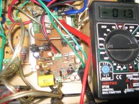
1st amp> has DC offset of 10mv
2nd amp> 1.3mv
1st amp> uses MPSA42/92, TIP41/42, output triples and MJ15003/4(for now 2 pairs)
2nd amp> uses BC546/556, TIP41/42, TIP35/36, MJE15030/31, output triples and MJ15003/4(for now 2 pairs)
(input sensitivity is same for both)
MOST important: Vbias has the normal cyclic variations when driving speakers (period of 30 minutes),
1st amp> varies from 2.40v to 2.88v (not good) but will tame this in the next weekend for sure
2nd amp> varies from 2.88v to 2.92v (good)
I have made a list of bad ideas which I tried and din’t work so learnt a lot and willing to try out new ideas soon.
Small NOTES for those wanting to try it out:
1> Always test your amp with low cost O/P device like 2N3055/MJ2955.
2> If connections are all fine but o/p heats or oscillates try increasing CDOM caps (if this Miller cap is too high then O/P will stick to half of +/- Vcc.
3> Don’t compromise on quality for dominant pole caps, first choice silver mica ( but I am using ceramic for now).
4> If the op stage is destroyed then replace the driver stage as well (domino effect).
5> If Vbias Iq is unstable, simplify VAS stage.
6> Test the amp completely and not just with Vas stage and closing the fb path.
My amp oscillates only when I lower the value of Cdom too low, so I stay put at 100pf and 1nf for 2 pole.
If I have 100 & 500pf it oscillates, if I want to use single pole I would go for 90pf or slightly lower. The power supply is +/-31V
I am yet to complete 2 more power amps which will drive my HF professional compression drivers,
For some more weeks these 2 amps will be on test bench and driving inexpensive 4 Ohm speakers and I am enjoying the music and getting good ideas to try out.
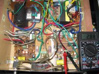
I have actually modified the circuit to get Vbias stability from the one publish in the Randy Slone’s book, if you are experienced you can make out from the photos and underneath the board I have power resistors 0.33E/5W and 2 tiny transistors to protect the VAS.
The reason I am using the output triples is that I am driving ancient O/P transistors in a EF. (also implementing feed forward circuit to Pre-driver stage as in Leach’s amp) Without output triples the amp turns on more smoothly, absolutely no thump. (though I am using turn on delay I measured the o/p)
I have few more experiment to complete and I am positive I will be able to lower the dc offset further for the 1st board.
output triples are really not necessary and I may remove it later after I try out few things.
I am not using 1 or 2 diodes in the fb path, the much better one is implementing bi-polar caps.
2 pole compensation is useful and I have tied them to ground. (if tying to Vcc then the resistor value may need experimenting)
Since I am doing all this on universal PCB I can’t afford any error with any of connections including op stage point to point connections or the temperature sense Bias transistors with it’s own circuits mounted on the OP Heat sink. So as I assemble I make sure it is 100% correct and I don’t find it taxing at the end to thoroughly review it.
Though I have solid experience with PCB design, layouts and ground routing, I am assembling this circuit on a universal PCB as I just need 4 power amps for my home and there are so many talented guys in this DIYAUDIO forum that I get my ideas from and willing to try it out myself which can never tire me out and it is all possible with the prototype board.
This design (dual differential input stage with current mirrors) is real stable and not dependant on High beta device. You would be surprised to see my videos (all more than 9MB) when I test it for the first time, there are thin wires (.6 mm) flying out everywhere (near the EI transformer, power cable, IP stage) but still it stays stable with no hum/hiss or any noise.
Slones’ super symmetrical current mirrors I/P stage are fantastic at the end!
The only loss I had so far while testing is one pair of blown op stage (2sc5200/2sa1943) & drivers, but this was at the beginning when I blindly tried out Slones’ design which dint have stable VAS current.
There is no components on the board running warm, the drivers used to run gently warm but after i put 100E as a base resistor I can barely feel the warmth. (I will remove this resistor soon)
This is fun and keeps the mind concentrated!
Till then bye and wish success!
Keep up the humor🙂
I am back with more success!
I have completed the second power amps on universal PCB with better performance than the first board!
To be short both amps don’t oscillate and are not tolerant to components or hfe variance!
Both amps tone/sonic sounds identical and I find absolutely no difference in listening test.
It is my favorite sounding amp so far.
1st amp> has DC offset of 10mv
2nd amp> 1.3mv
1st amp> uses MPSA42/92, TIP41/42, output triples and MJ15003/4(for now 2 pairs)
2nd amp> uses BC546/556, TIP41/42, TIP35/36, MJE15030/31, output triples and MJ15003/4(for now 2 pairs)
(input sensitivity is same for both)
MOST important: Vbias has the normal cyclic variations when driving speakers (period of 30 minutes),
1st amp> varies from 2.40v to 2.88v (not good) but will tame this in the next weekend for sure
2nd amp> varies from 2.88v to 2.92v (good)
I have made a list of bad ideas which I tried and din’t work so learnt a lot and willing to try out new ideas soon.
Small NOTES for those wanting to try it out:
1> Always test your amp with low cost O/P device like 2N3055/MJ2955.
2> If connections are all fine but o/p heats or oscillates try increasing CDOM caps (if this Miller cap is too high then O/P will stick to half of +/- Vcc.
3> Don’t compromise on quality for dominant pole caps, first choice silver mica ( but I am using ceramic for now).
4> If the op stage is destroyed then replace the driver stage as well (domino effect).
5> If Vbias Iq is unstable, simplify VAS stage.
6> Test the amp completely and not just with Vas stage and closing the fb path.
My amp oscillates only when I lower the value of Cdom too low, so I stay put at 100pf and 1nf for 2 pole.
If I have 100 & 500pf it oscillates, if I want to use single pole I would go for 90pf or slightly lower. The power supply is +/-31V
I am yet to complete 2 more power amps which will drive my HF professional compression drivers,
For some more weeks these 2 amps will be on test bench and driving inexpensive 4 Ohm speakers and I am enjoying the music and getting good ideas to try out.
I have actually modified the circuit to get Vbias stability from the one publish in the Randy Slone’s book, if you are experienced you can make out from the photos and underneath the board I have power resistors 0.33E/5W and 2 tiny transistors to protect the VAS.
The reason I am using the output triples is that I am driving ancient O/P transistors in a EF. (also implementing feed forward circuit to Pre-driver stage as in Leach’s amp) Without output triples the amp turns on more smoothly, absolutely no thump. (though I am using turn on delay I measured the o/p)
I have few more experiment to complete and I am positive I will be able to lower the dc offset further for the 1st board.
output triples are really not necessary and I may remove it later after I try out few things.
I am not using 1 or 2 diodes in the fb path, the much better one is implementing bi-polar caps.
2 pole compensation is useful and I have tied them to ground. (if tying to Vcc then the resistor value may need experimenting)
Since I am doing all this on universal PCB I can’t afford any error with any of connections including op stage point to point connections or the temperature sense Bias transistors with it’s own circuits mounted on the OP Heat sink. So as I assemble I make sure it is 100% correct and I don’t find it taxing at the end to thoroughly review it.
Though I have solid experience with PCB design, layouts and ground routing, I am assembling this circuit on a universal PCB as I just need 4 power amps for my home and there are so many talented guys in this DIYAUDIO forum that I get my ideas from and willing to try it out myself which can never tire me out and it is all possible with the prototype board.
This design (dual differential input stage with current mirrors) is real stable and not dependant on High beta device. You would be surprised to see my videos (all more than 9MB) when I test it for the first time, there are thin wires (.6 mm) flying out everywhere (near the EI transformer, power cable, IP stage) but still it stays stable with no hum/hiss or any noise.
Slones’ super symmetrical current mirrors I/P stage are fantastic at the end!
The only loss I had so far while testing is one pair of blown op stage (2sc5200/2sa1943) & drivers, but this was at the beginning when I blindly tried out Slones’ design which dint have stable VAS current.
There is no components on the board running warm, the drivers used to run gently warm but after i put 100E as a base resistor I can barely feel the warmth. (I will remove this resistor soon)
This is fun and keeps the mind concentrated!
Till then bye and wish success!
Keep up the humor🙂
Attachments
Smathias,
Your performances really keeps me Baffled. I am happy for you it works as you like it but I went to so many troubles with that VAS Iq that I gave up doing it that way. I am going to try the CMCL as you can read. In the end it is the same layout as yours as Slones but with an active part to control the VAS Iq ...
Thanks for sharing your findings and trial logs I think people should do that all the time instead of us inventing all warm water again or inventing the wheel over and over again !
Keep up the work dude !
Edmond,
I just read your reply... I will look more deeply into it next and let you know soon !!
About cascoding as you know I have a magical feeling about them, they are my fetisch 🙂 Even if the simulation shows some THD rise, I believe this to be small and most of all 'theoretical', as in real life the 'gain' of inserting them might be bigger than the 'loss'. However let me check it out on the sim too ...
About the VAS Iq, I simulated so much times, and 20 to 30mA seems to be perfect for THD. If you check the SOA of the devices, 20mA @ say 80V should be OK with some heatsinking... If the the OPS has a Zin of 10K the current load for the VAS on top of DC is going to be say 80V / 10K or 8mA + 20mA DC = max 30mA AC+DC. I Use 6,90°C/W Heatsinks for them. The AC part is only so large if the amp is used full power and the signal is at least intermittend ... Do I overlook something? by the way : that 20K load is a simulation as if the ops would load the VAS ... 10K , 20K whatever it will be ... according to Slone more like 10K for mosfet and down to 1K for BJT, depending on driver stages...
I need to investigate further on that TMC THD rise ... but it costs nothing to route a resistor to VCCs so one could still check in real life the difference between TMC and TPC. It would be nice to test THD and other stuff from the same AMP with just displacing the resistor from the power rails end to the feedback rail...
I was going for SOURCE FOLLOWERS for simplicity but reading books it seems CF shows OPS THD 5 to 10 times lower than SF or EF ... but then again I definitly do not want to run into HF problems because I am tired to VOODOO my Q's 🙂 and MOSFETS are more prone to RF problems... so source followers it will be.
The rest I'll check out ...
No more double Whammy's for me ... just big Macs 🙂
Bye
Olivier
Hi Olivier,
I finished experimenting with Vbe multiplier,
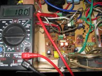
The 2 transistor version (Sziklai pair) goes very well with my amp, the Vbias variance is absolutely not there. I have tested for an hour with medium power music, it stays 2.39 to 2.40V . There is no instability with this feedback loop - Vbe multiplier even when I was doing the test the way shown in the photos.
I implemented this on my power amp board-1, on which Vbias used to drift , though the drift was due to poorer transistors (TIP41/42C) configured as output triples. After implementing this without any modification to the amp the variance is controlled tight.
Sharing Notes:
1>Do not go too low with the resistors (less than 200E) high voltage turns up everywhere in almost all components. (but voltage across Vbias E & C will show zero)
2>BD 139/BD 140 not satisfactory
3.Strongly recommend Sziklai pair- Vbe multiplier for Slones Amp
Two accidents happened while testing, usually I am very careful but this happened late during midnight)
While testing the VBe multiplies the entire negative connecting wire (Collector of 2nd pair) was not connected to the Amp!
The O/P transistors heated rapidly and could hear the transforms jerk BUT THIS AMP SURVIVED!! (strange the 5 A fuse dint die)
The next one was, I was testing all this on real one pair power output transistors and the other pair emitters removed, one of this wire slipped and shorted with Ground, again nothing happened it Survived!
WOW ! Are these transistors Mj15003/4 indestructible?
Smathias
I finished experimenting with Vbe multiplier,
The 2 transistor version (Sziklai pair) goes very well with my amp, the Vbias variance is absolutely not there. I have tested for an hour with medium power music, it stays 2.39 to 2.40V . There is no instability with this feedback loop - Vbe multiplier even when I was doing the test the way shown in the photos.
I implemented this on my power amp board-1, on which Vbias used to drift , though the drift was due to poorer transistors (TIP41/42C) configured as output triples. After implementing this without any modification to the amp the variance is controlled tight.
Sharing Notes:
1>Do not go too low with the resistors (less than 200E) high voltage turns up everywhere in almost all components. (but voltage across Vbias E & C will show zero)
2>BD 139/BD 140 not satisfactory
3.Strongly recommend Sziklai pair- Vbe multiplier for Slones Amp
Two accidents happened while testing, usually I am very careful but this happened late during midnight)
While testing the VBe multiplies the entire negative connecting wire (Collector of 2nd pair) was not connected to the Amp!
The O/P transistors heated rapidly and could hear the transforms jerk BUT THIS AMP SURVIVED!! (strange the 5 A fuse dint die)
The next one was, I was testing all this on real one pair power output transistors and the other pair emitters removed, one of this wire slipped and shorted with Ground, again nothing happened it Survived!
WOW ! Are these transistors Mj15003/4 indestructible?
Smathias
Attachments
Hi Edmond,
I adapted the schematic on a few points. First of all, I reduced Iq VAS down to 7mA approximately. I implemented TPC and TMC setting one resistor to the correct value while the other is raised to 10Meg. In reality the non serving one won't be soldered onto the pcb. I included your clamps also in the VAS. I kept the cascoded VAS and I kept the protection for VAS Iq in the cascode leg. Maybe that can still be changed, I kept it there because otherwise we need to keep a resistance in the emitter leg of the VAS amplifier Q's which in turn loads the IS with input impedance, but since the CMCL requires a resistor there too, it's another ball game. I'll see that later.
I modified slightly the routing for the rail voltages, which is not of concern in the schematic, but just to remember me later when doing the pcb. I also inluded a second set of decoupling caps.
Implemented the Zobel network.
Included some caps around the Mosfets as you can see. However I copied this from other schematics and don't really know their influence...I believe it must be RF rejection related....
Adjusted rail potential, but this doesn't matter.
Some questions however :
- why did you install C22 and C23? They seem switch-off capacitors to me, but do L-Mosfets suffer from switching distortion or is this to be versatile in case of changing to BJT's? Or is it something else?
- You mentionned searching for good Driver transistor, well I found the KSA1220 or 2SA1220 but except for better power characterisitcs they are not as good as the the KSA1381 or 2SA1381. If the latter are just used to drive 2 Mosfet stages this should suffise no? No use for changing to heavier drivers right?
- I notice that 1KHZ THD is really low : under 4u%, but at 20KHZ it rises to 800u% which is not bad but it is a big raise anyway, so looking deeper into it I see that the raise is primarily due to higher order harmonics like the 11th and 13th for instance...Of course this is over 200KHZ does it really matter? What is the source for this? Vbias induced high order harmonics?
- I worry about the nyquist stability Vout (before Zobel) compared to Vin inverting differential input show a phase lag of nearly 200° where the magnitude (amped) becomes 0. However if I compare the phase lage between Vin diff + and Vin diff - it is 0° all the way and around the magnitude zero point the lag shows a downward spike going to -50° ... what counts as nyquist stability???
See plots
I still need to incorporate a protection circuit for the OPS ! What do you think of it? Simple VI limiter? Single slope? dual slope? multi slope?
Damn its late i go to sleep
Greetz
Olivier
Attachments
Hi Edmond,
I adapted the schematic on a few points. First of all, I reduced Iq VAS down to 7mA approximately.
Hi Olivier,
With 7mA the PD is still quit high. Why not reduce it to say 5mA? You don't need that much current.
I implemented TPC and TMC setting one resistor to the correct value while the other is raised to 10Meg. In reality the non serving one won't be soldered onto the pcb. I included your clamps also in the VAS. I kept the cascoded VAS and I kept the protection for VAS Iq in the cascode leg. Maybe that can still be changed, I kept it there because otherwise we need to keep a resistance in the emitter leg of the VAS amplifier Q's which in turn loads the IS with input impedance, but since the CMCL requires a resistor there too, it's another ball game. I'll see that later.
If you don't mind to blow another bunch of trannies, just keep the protection there.
But I strongly advice you to change that. See the schematics below. This time I've done it in a slightly different way: instead of sensing the emitter resistor of the VAS itself, now the emitter resistor of the VAS-copy is sensed. Same results of course, but the schematic (and probably the PCB as well) looks a bit 'nicer'.
I modified slightly the routing for the rail voltages, which is not of concern in the schematic, but just to remember me later when doing the pcb. I also included a second set of decoupling caps.
Implemented the Zobel network.
Okay.
Included some caps around the Mosfets as you can see. However I copied this from other schematics and don't really know their influence...I believe it must be RF rejection related....
I'm not sure whether they are really needed, though it doesn't harm. Better safe then sorry
Adjusted rail potential, but this doesn't matter.
Some questions however :
- why did you install C22 and C23? They seem switch-off capacitors to me, but do L-Mosfets suffer from switching distortion or is this to be versatile in case of changing to BJT's? Or is it something else?
You are right. They are switch-off capacitors. Maybe you don't need them in case of laterals, but certainly in case of vertical MOSFETs and BJTs.
The trouble with this kind of topology is that the driver turns the MOSFETs faster on than off. Those capacitors partly cured the problem. But if you like to do it really nice, then use 'split' drivers, i.e. the 'top' respectively 'bottom' MOSFETs are driven by their 'own' push-pull driver. Then you don't need those caps at all, which creates another problem in return. See also my next comment
- You mentioned searching for good Driver transistor, well I found the KSA1220 or 2SA1220 but except for better power characteristics they are not as good as the the KSA1381 or 2SA1381. If the latter are just used to drive 2 Mosfet stages this should suffice no? No use for changing to heavier drivers right?
But two MOFETS pairs (in particular laterals) isn't enough. Four pairs is far better. However, in that case you will need indeed a more powerful driver. That means two pair of SA1381/KSC3503. But instead of using them simply in parallel (as show in my previous schematic), it's even better to use the same number of trannies in the aforementioned split driver approach. The only thing that complicates the design a bit, are the two bias generators needed for the push-pull drivers (two more trannies)
- I notice that 1KHZ THD is really low : under 4u%, but at 20KHZ it rises to 800u% which is not bad but it is a big raise anyway, so looking deeper into it I see that the raise is primarily due to higher order harmonics like the 11th and 13th for instance...Of course this is over 200KHZ does it really matter? What is the source for this? Vbias induced high order harmonics?
First, the THD sim is very inaccurate, mainly as a result of poor modeling of the lateral MOSFETs.
Second, as already pointed out, THD will rise considerably with frequency: with 3rd power!
(or 18dB/octave). So this increase is not bad at all.
BTW, if you don't like this behavior, the only thing you can do about it is increasing the distortion at lower frequencies. Although propagated by some alleged audio gurus, this is of course the most stupid thing ever.
- I worry about the nyquist stability Vout (before Zobel) compared to Vin inverting differential input show a phase lag of nearly 200° where the magnitude (amped) becomes 0. However if I compare the phase lage between Vin diff + and Vin diff - it is 0° all the way and around the magnitude zero point the lag shows a downward spike going to -50° ... what counts as nyquist stability???
See plots
You can't assess the loop response in this way. Please use the method as shown in: CMCL-global-loop-gain.cir
Of course you need some kind of protection. I would recommend a simple current limiter. No VI limiter, as the positive voltage feedback tends to destabilize the limiter.I still need to incorporate a protection circuit for the OPS ! What do you think of it? Simple VI limiter? Single slope? dual slope? multi slope?
Damn its late i go to sleep
Greetz
Olivier
One more thing, the voltage clamp in my previous schematic is totally wrong. I don't know how and why this happened. Probably during a redraw/cleanup. My apologies for this gross error. Below are the correct circuits (with and without cascode).
Next time I will show you an example with split drivers. That will take a few days as many other things have to be changed as well.
Groeten,
Edmond.
Attachments

Hi Bonsai,
Perhaps it looks nice, but my sim doesn't show any improvement. Probably because the adverse effects of Cob and Mr Early have already been remedied by the so called 'beta enhancement trannies' in front of the VASes.
OTOH, I'm glad that I can omit these additional components.The simpler the better.
@ Olivier,
Could you measure the real Vgs @ Id = 100mA of your laterals, please?
If too low (<0.7V), it will complicate the new design
Regards,
Edmond.
Perhaps it looks nice, but my sim doesn't show any improvement.
Probably because the adverse effects of Cob and Mr Early have already been remedied by the so called 'beta enhancement trannies' in front of the VASes.OTOH, I'm glad that I can omit these additional components.The simpler the better.
@ Olivier,
Could you measure the real Vgs @ Id = 100mA of your laterals, please?
If too low (<0.7V), it will complicate the new design
Regards,
Edmond.
Edmond,
I lowered the VAS Iq down to 5.7mA now. Same THD anyway in the sim.
No problem to change the location of the VAS protection from the Cascode Leg to the VAS leg. I would like to know if it is really a good idea to put it on the copy of the VAS Iq? It should work since it is a copy, but what if a failure causes the VAS Iq to climb sky high AND also destroys the tracking circuit between the VAS Iq and its copy at the same time ... it won't protect right? The same is true the other way around but basicly it might be better to be safe on the real VAS Iq instead of its copy...right or wrong? One could protect both too but this might be an overkill ... ok I moved it there anyway ...
I didn't understand the explanation about the drivers I guess. Let me tell you what I read : Slone connects the sourcefollowers L-MOSFETS directly to the VAS stage, this explains maybe why the VAS Iq is so high!? He uses those famous 2SD669 and 2SB649 which are hard to find and also hard to get spice models for! But ok, apart from that is it not good to drive 2 times 2 mosfet pairs with those 2sa1381 like in the last circuit i uploaded yesterday? each driver pair only needs to feed a dual pair of mosfets...? Is going to the burden of pushpulling drivers and dual vbias worth the results? Our circuit is already becoming a factory ! 🙂 As for the switchoff caps ... I have to admit this ops stuff is going over my head but I am happy to hear your propositions for the next step in this...
Increasing LF THD just to create an illusion it rises less at higher frequencies is really stupid !
I will check the phase stuff with the other method you told me and you know if things are stable or not
Wouldn't a simple I limiter restrict the amps power too much?
I will change the clamp circuit , but are you using tunnel diodes now? Gee Edmond, this circuit is becomming complex ... you should pattent it 🙂 If it works 🙂)))
I'll post the modified circuit soon...
for now bye bye
Olivier
Edmond,
I lowered the VAS Iq down to 5.7mA now. Same THD anyway in the sim.
No problem to change the location of the VAS protection from the Cascode Leg to the VAS leg. I would like to know if it is really a good idea to put it on the copy of the VAS Iq? It should work since it is a copy, but what if a failure causes the VAS Iq to climb sky high AND also destroys the tracking circuit between the VAS Iq and its copy at the same time ... it won't protect right? The same is true the other way around but basicly it might be better to be safe on the real VAS Iq instead of its copy...right or wrong? One could protect both too but this might be an overkill ... ok I moved it there anyway ...
Hi Olivier,
You made me thinking, thanks! Initially, the protection was only meant against excessive large input signals. In that case it doesn't matter which VAS is protected; the VAS itself or its 'clone'.
BUT in case of a component failure, it's indeed far better to protect the VAS itself. Imagine what would happen if the bias generator is blown to an open circuit? Bye bye OPS!
I didn't understand the explanation about the drivers I guess. Let me tell you what I read : Slone connects the source followers L-MOSFETS directly to the VAS stage, this explains maybe why the VAS Iq is so high!? He uses those famous 2SD669 and 2SB649 which are hard to find and also hard to get spice models for!
If you input a 1V (2V pk-pk) square wave, the gates (4 pairs) needs some 100mA (peak) drive current. Only a heavy industrial VAS is capable to supply such large currents. So, don't listen to Mr Slone, please. You better listen to Bob Cordell, as he once said: 'it's crazy to not use a driver'.
But ok, apart from that is it not good to drive 2 times 2 mosfet pairs with those 2sa1381 like in the last circuit i uploaded yesterday? each driver pair only needs to feed a dual pair of mosfets...? Is going to the burden of pushpulling drivers and dual vbias worth the results? Our circuit is already becoming a factory ! 🙂
That's right. It's becoming fairly complex. If you ask for quality, you have to pay attention to every detail. Hence the increased complexity. There ain't no free lunch.
As for the switch-off caps ... I have to admit this ops stuff is going over my head but I am happy to hear your propositions for the next step in this...
Indeed. This is quite a complicated matter. In short, if the amp is subjected to a large HF sine or square wave, the voltage across these caps will increase. As a result, the bias of the OPS will increase too (we don't want this). But at the same time the standing current of the driver stage will decrease. It's the latter that might cause serious trouble, as at low currents, gm and fT decrease also, which causes (in some cases) instability.
Increasing LF THD just to create an illusion it rises less at higher frequencies is really stupid !
Interestingly, if the circuit includes the OPS, the THD increase is far less pronounced. As for the attached circuit, only 46 times from 1kHz to 20kHz. Probably, this might be explained by the fact that the OPS is the main cause or distortion (hence a less steeper rise with frequency), though I'm not sure.
I will check the phase stuff with the other method you told me and you know if things are stable or not
Wouldn't a simple I limiter restrict the amps power too much?
Yes, indeed. But I don't know a better solution. I opt for stability instead of economy. This DIY, you know. 😉
I will change the clamp circuit , but are you using tunnel diodes now?
No?! the BAV21 is just a high voltage diode (200V).
Gee Edmond, this circuit is becoming complex ... you should patent it 🙂 If it works 🙂)))
Yes it works (CMCL), see the PGP amp.
In Europe, patents are way too expensive. In this niche market you will never earn the huge investment back.
I'll post the modified circuit soon...
Me first. 😀
for now bye bye
Olivier
Below a first attempt to incorporate the split driver approach. Notice the zero volt bias generator (the wiper of X1 is set to 0%)! This is because Vgth is sooooo low. Temperature compensation and OPS bias is provided by Q26 & Q27, which should be mounted on the main heat sink.
The bias generators for the split drivers consist of Q23 & Q24. Simple isn't it.
The constant current sources has been made more stable, as a lot of other things depends on them.
You can also use this file as template for future designs, as it contains some convenient definitions to do a THD analysis at different frequencies (go the 'text page' and modify .define ff 20e3).
Run the DC analysis to see the start-up behavior (no 'thump')
Gegroet,
Edmond.
Attachments
Hi Olivier,
Here a second attempt. Main differences are:
- Higher emitter resistors of the input stage, because the ULGF was too high. Now it's 1.5MHZ.
- NFB voltage clamp, as the previous one was a little bit unstable (ringing)
- Provisions for ultra low Vgth MOSFETS
- Fast acting over-current protection.
- Provisions for a slow acting over-current protection (not fully implemented yet).
- Different roll-off method for the CMCL (better step response)
Gegroet,
Edmond.
Attachments
Last edited:
Please test your amp without beta-enhancer first,
if it works perfect then include the beta-enhancer but with HIGH value for R32 (emitter resistor for Q21).
When it works out fine then fix the calculated value for R32.
Make all provision for Beta-enhancer in your PCB design but test it stage by stage.
I am not using Beta-enhancer in my amp but a simple current buffer before VAS, which is effective but the test is not complete. This enhances the tone of music, the vocals sounds good & better.
It has no problem as associated with beta enhancer. I have given safety margin for buffer resistors, if I go too low then the amp picks up parasitic. I am not using any base stopper any where just at the bases of OP power transistors (4.7E)
I am able to make the difference as I compare the 2 amps which is under test and hammer, one amp is used as reference and the other undergoes all ideas.
Did you know single or 2 pole CDOM caps make no changes to the tone, but at high volume or power OP the distortion is less especially with low frequency. (somebody wanted to know about this in this DIY forum)
Patent 5635874 is a good read
Attachments
- Home
- Amplifiers
- Solid State
- HEEEELLLPPP : M. Randy Slone Mirror Image Topology Construction - Troubles