Same at the schematics of ecdesigns ?
No, EC's schematic is correct.
For TDA1541A, BCK determines the exact moment the input latch data is transferred to the output latch (and a new sample is output). This happens at the first positive going edge of BCK, after WS has gone low. So BCK needs to have lowest jitter as it directly relates to output sample timing jitter.
All I2S signals must be attenuated to approx. 200mVpp. This reduces I2S input circuit ground-bounce (current steering inputs), and results in a more detailed and refined sound.
DEM clock is required to drive the switch matrix, part of active current dividers. The DEM clock basically changes switch matrix position (4-way electronic switches) after each DEM clock pulse. The TDA1541A has an on-chip DEM oscillator that requires one external capacitor (usually around 470 ... 560pF).
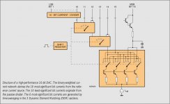
I attached a Philips block diagram illustrating DEM operation. The block "shiftregister" is connected to the DEM oscillator. DEM circuit provides 4 closely matched (time averaging) active divider output currents. This in turn increases DAC (long term) accuracy.
problem is that the DEM clock has crosstalk with BCK (on-chip) and BCK and DEM clock will inter-modulate, causing sound quality degradation. The 14 active divider decoupling caps need to have lowest inductance, very low leakage current, and must be connected using shortest possible wiring. This basically means they have to be placed underneath the DAC chip, so they must be very small. I suggest PPS or PEN 1206 film caps (47nF), these are also very good for power supply decoupling.
In order to prevent BCK and DEM clock from inter-modulating (and degrading sound quality), both BCK and DEM should either have same frequency, or they should run in perfect sync. I plan to use 1.4112 MHz DEM / BCK clock in my new TDA1541A module for the ISD player.
I currently use a 13K resistor in series with a BAT43 (Schottky diode). The BAT43 anode connects to a 2Vpp 1.4112 MHz clock, the cathode connects to the resistor. The resistor connects to pin 16 (pin 17 remains unconnected).
About reclocking,
Using a virtually perfect digital audio source (SD-transport), it's clearly audible that every added clock load further degrades sound quality, no matter how well the clock is buffered. Buffers increase jitter and indirectly degrade master clock performance. My personal conclusion is to reduce the amount of clock loads to absolute minimum.
I use one synchronous reclocker for BCK, it's integrated in the master clock in order to minimize trace length and enabling use of capacitive node. This capacitive node enables clocking the flip-flop using a clean un-buffered and filtered clock output. This guarantees extreme low jitter levels. The capacitive node places approx. 0.1pF clock load on the master clock.
Dividers contain multiple flip-flops, this will produce more switching noise / jitter compared to a single D flip-flop. So I no longer use divider circuits.
The buffered master clock output is used to drive one more clock load (digital audio source). So I now use two clock loads that are connected at different ponts on the master clock. The synchronous reclocker is clocked by an un-buffered filtered clock signal (pure sine wave with approx. 20Vpp amplitude), and a buffered clock signal (approx. 6Vpp signal with fast positive going transients and slow negative going transients) for clocking (slaving) the SD-transport.
Good voltage regulator alone is not sufficient for powering an ultra low jitter clock. I had to use a local shunt reg (2 x 2V) on the master clock, and a 20th order LC low pass power supply filter (10 x 3.3mH and 10 x 1200uF). The actual 5.4V power supply feeding the LC filter has 3-stage stepped rectifiers, 9V discrete series pre-regulator, followed by a 5.4V discrete post regulator with complementary output (PNP / NPN Darlington stage). This power supply concept just managed to achieve desired results.
It's also important to minimize loop current of the connected digital audio source, this can be done by using maximum possible series impedance. This is so critical that the series resistor properties directly affect sound quality. It turned out that both multiple resistors in series (6 x 330R for example) or (multiple) bulk metal foil resistors offer best results. This is caused by the reduced self capacitance, Bulk metal foil is specified at <1pF, and placing multiple resistors in series, reduces self capacitance by placing self capacitances in series).
Final tip, keep digital (clock) signal path as simple as possible using fewest parts as possible in the signal path. Also try to use lowest possible clock frequencies for clocking the DAC chip (BCK). I now use 1.4112 MHz bit clock, this is possible by using 32 bits / frame instead of 64 bits / frame that would require 2.8224 MHz bit clock.
It will work, but when you read above explanation, you will notice that this approach doesn't allow ultimate performance (multiple dividers plus an extra D flip-flop).
All I2S signals must be attenuated to approx. 200mVpp. This reduces I2S input circuit ground-bounce (current steering inputs), and results in a more detailed and refined sound.
DEM clock is required to drive the switch matrix, part of active current dividers. The DEM clock basically changes switch matrix position (4-way electronic switches) after each DEM clock pulse. The TDA1541A has an on-chip DEM oscillator that requires one external capacitor (usually around 470 ... 560pF).
I attached a Philips block diagram illustrating DEM operation. The block "shiftregister" is connected to the DEM oscillator. DEM circuit provides 4 closely matched (time averaging) active divider output currents. This in turn increases DAC (long term) accuracy.
problem is that the DEM clock has crosstalk with BCK (on-chip) and BCK and DEM clock will inter-modulate, causing sound quality degradation. The 14 active divider decoupling caps need to have lowest inductance, very low leakage current, and must be connected using shortest possible wiring. This basically means they have to be placed underneath the DAC chip, so they must be very small. I suggest PPS or PEN 1206 film caps (47nF), these are also very good for power supply decoupling.
In order to prevent BCK and DEM clock from inter-modulating (and degrading sound quality), both BCK and DEM should either have same frequency, or they should run in perfect sync. I plan to use 1.4112 MHz DEM / BCK clock in my new TDA1541A module for the ISD player.
I currently use a 13K resistor in series with a BAT43 (Schottky diode). The BAT43 anode connects to a 2Vpp 1.4112 MHz clock, the cathode connects to the resistor. The resistor connects to pin 16 (pin 17 remains unconnected).
About reclocking,
Using a virtually perfect digital audio source (SD-transport), it's clearly audible that every added clock load further degrades sound quality, no matter how well the clock is buffered. Buffers increase jitter and indirectly degrade master clock performance. My personal conclusion is to reduce the amount of clock loads to absolute minimum.
I use one synchronous reclocker for BCK, it's integrated in the master clock in order to minimize trace length and enabling use of capacitive node. This capacitive node enables clocking the flip-flop using a clean un-buffered and filtered clock output. This guarantees extreme low jitter levels. The capacitive node places approx. 0.1pF clock load on the master clock.
Dividers contain multiple flip-flops, this will produce more switching noise / jitter compared to a single D flip-flop. So I no longer use divider circuits.
The buffered master clock output is used to drive one more clock load (digital audio source). So I now use two clock loads that are connected at different ponts on the master clock. The synchronous reclocker is clocked by an un-buffered filtered clock signal (pure sine wave with approx. 20Vpp amplitude), and a buffered clock signal (approx. 6Vpp signal with fast positive going transients and slow negative going transients) for clocking (slaving) the SD-transport.
Good voltage regulator alone is not sufficient for powering an ultra low jitter clock. I had to use a local shunt reg (2 x 2V) on the master clock, and a 20th order LC low pass power supply filter (10 x 3.3mH and 10 x 1200uF). The actual 5.4V power supply feeding the LC filter has 3-stage stepped rectifiers, 9V discrete series pre-regulator, followed by a 5.4V discrete post regulator with complementary output (PNP / NPN Darlington stage). This power supply concept just managed to achieve desired results.
It's also important to minimize loop current of the connected digital audio source, this can be done by using maximum possible series impedance. This is so critical that the series resistor properties directly affect sound quality. It turned out that both multiple resistors in series (6 x 330R for example) or (multiple) bulk metal foil resistors offer best results. This is caused by the reduced self capacitance, Bulk metal foil is specified at <1pF, and placing multiple resistors in series, reduces self capacitance by placing self capacitances in series).
Final tip, keep digital (clock) signal path as simple as possible using fewest parts as possible in the signal path. Also try to use lowest possible clock frequencies for clocking the DAC chip (BCK). I now use 1.4112 MHz bit clock, this is possible by using 32 bits / frame instead of 64 bits / frame that would require 2.8224 MHz bit clock.
can you confirm that this circuit TDA1541 DEM reclocking will work
It will work, but when you read above explanation, you will notice that this approach doesn't allow ultimate performance (multiple dividers plus an extra D flip-flop).
Attachments
Hello ecdesigns,
many thanks for growing that DEM stuff out of you!
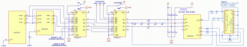
I will try the DEM-synchronization by chip first bevore your version with injekting over shottky and resistor. First bevore trying i will ask if the embed of the 74HC74 in the attachment is doing right.
Q1: can you confirm that this circuit TDA1541 DEM reclocking will work?
Q2: wich effekt will have to change the TDA 16 and 17 (16 to Q and 17 to /Q against 16 to /Q and 17 to Q) in this circuit?
many thanks for growing that DEM stuff out of you!
I will try the DEM-synchronization by chip first bevore your version with injekting over shottky and resistor. First bevore trying i will ask if the embed of the 74HC74 in the attachment is doing right.
Q1: can you confirm that this circuit TDA1541 DEM reclocking will work?
Q2: wich effekt will have to change the TDA 16 and 17 (16 to Q and 17 to /Q against 16 to /Q and 17 to Q) in this circuit?
Attachments
Last edited:
and prevent DEM clock with our music from inter-modulating you need good decoupling of DEM currentsIn order to prevent BCK and DEM clock from inter-modulating
Its depend on type of oscillatorGood voltage regulator alone is not sufficient for powering an ultra low jitter clock
and prevent DEM clock with our music from inter-modulating you need good decoupling of DEM currents
Yes you are correct,
I now plan to use 1206 size PPS or PEN SMD film caps that will be mounted underneath the TDA1541A in order to provide shortest possible connections. The tiny SMD parts use stacked foil construction and should have low inductance (more effective decoupling).
Active divider decoupling caps don't fully prevent crosstalk between DEM clock and bit clock. That's why I decided to use same frequency for both bit and DEM clock. This eliminates on-chip inter-modulation as both frequencies run in exact phase and have same frequency
I also plan to use two dedicated decoupling cap GND return paths, one for each channel. This also prevents interference with GND supply currents that might be super-imposed on the decoupling cap GND traces. This in turn keeps the active divider output currents as clean as possible.
Highest available value (1206) film cap is around 47nF/16V (AVX / Panasonic). This should be sufficient when using 8 times higher DEM clock frequency (1.4112 MHz).
Its depend on type of oscillator
Each (crystal) oscillator has certain PSRR and might benefit from a cleaner power supply, resulting in even lower jitter. The 4-crystal superclock I am using has approx. 40 times higher PSRR compared to most audiophile master clocks, and it keeps performing even better when power supply noise is further reduced. As far as I have been able to test, lowest possible jitter (preferably zero) provides best results.
good progress, i use 1206 underbody many years, it gives excellent results, but PEN or PPS have strong soldering thermal layout, and in this place lose X7R, NP0 (better ESL, ESR, capacity = lower impedance)I now plan to use 1206 size PPS or PEN SMD film caps that will be mounted underneath the TDA1541A in order to provide shortest possible connections.
if caps with right capacity,ESR,ESL - completely.Active divider decoupling caps don't fully prevent crosstalk between DEM clock and bit clock
statistical averaging. Philips engineers were not fools 🙂I decided to use same frequency for both bit and DEM clock. This eliminates
not sufficient 🙁This should be sufficient when using 8 times higher DEM clock frequency (1.4112 MHz).
output jitter - PSU noise depends on the oscillator type, ECL, CMOS, Colplitz discrete etc, one oscillator need very low noise PSU, other not, both with the same output jitterEach (crystal) oscillator has certain PSRR and might benefit from a cleaner power supply, resulting in even lower jitter
Jitter value - sonic performance completely depends on the jitter spectrum and dac type used.As far as I have been able to test, lowest possible jitter (preferably zero) provides best results.
Last edited:
...
Highest available value (1206) film cap is around 47nF/16V (AVX / Panasonic).
Panasonic ECPU1C684MA5, PPS, 680nF PANASONIC|ECPU1C684MA5|CAPACITOR, 0.68UF, 16V | Farnell United Kingdom
Kemet C1210C224J3GAC, NP0(C0G), 1210, 220nF Your Search Results | Farnell United Kingdom

has someone compared this from CD 9009?
Hi nanocamp,
i will try to check the Grundig solution. Because i have got the top-board out of my Tube-DAC to check my psu and shunt modules,
i could also test this soluton for the DEM-reclocking. I think it is very similar to the actual solution from -ecdesigns-.

Hi, I just tried this in my DAC. Wow what an improvement. I only had the capacitor between pins 16 & 17. I am going to make this a permanent mod. Tight base and cleaner treble.has someone compared this from CD 9009?
Regards, John
John Hi
Can you widen this out a bit.
You put a capacitor across 16 and 17.......along with the DEM clock mods ?
I read the nanocamp bit but can not fathom out what you mean.
Can you widen this out a bit.
You put a capacitor across 16 and 17.......along with the DEM clock mods ?
I read the nanocamp bit but can not fathom out what you mean.
Hi, What I meant was I only had the capacitor between pins 16 & 17 until I did the modification Re: CD 9009. I did what was shown in the CD 9009 schematic.John Hi
Can you widen this out a bit.
You put a capacitor across 16 and 17.......along with the DEM clock mods ?
I read the nanocamp bit but can not fathom out what you mean.
Regards, John
What diode and caps did you choose? I have been following Andrew's experience ... also very favourable.
Hi, I didn't use anything special. Philips 6v2 zenner with two 100n smt caps and a metal film resistor.What diode and caps did you choose? I have been following Andrew's experience ... also very favourable.
Regards, john
John Hi
Sorry for the delay in replying.
Your cap comment on the 20th May started the whole thing off for me
and it
Sorry for the delay in replying.
Your cap comment on the 20th May started the whole thing off for me
and it
What happened there ?
I was thanking you for posting that comment on the 20th May.
It started my curiosity to the point where I tried it and agreed with you completely.
I've since gone a little further but it's down to you - many thanks
Andrew
I was thanking you for posting that comment on the 20th May.
It started my curiosity to the point where I tried it and agreed with you completely.
I've since gone a little further but it's down to you - many thanks
Andrew
I don't see the point of WS frequency equal to DEM frequency. Shouldn't it be 4x, 8x, 12x, or even 16x the WS frequency?has someone compared this from CD 9009?
Should it be synchronous to WS at all? I am thinking of trying a digital PRBS (Pseudo Random Binary Sequence) generator for driving the DEM circuit.
I don't see the point of WS frequency equal to DEM frequency. Shouldn't it be 4x, 8x, 12x, or even 16x the WS frequency?
Should it be synchronous to WS at all? I am thinking of trying a digital PRBS (Pseudo Random Binary Sequence) generator for driving the DEM circuit.
With typical 4 times oversampling, WS frequency would equal 4 x 44.1 KHz = 176 KHz. This falls within datasheet DEM oscillator frequency specs. When running the TDA1541A in NOS, WS frequency equals 44.1 KHz, this DEM frequency is too low.
The reason the DEM clock must be synchronous with the I2S timing signals is that there is on-chip crosstalk between I2S timing signals and DEM logic. This can be proven by tuning the DEM oscillator cap (trimmer), on a certain moment the DEM oscillator will "lock" to the bit clock, this is only possible when there is sufficient crosstalk between bit clock and DEM oscillator.
When the DEM clock is not synchronized with the I2S timing signals, both DEM clock and I2S timing signals will inter-modulate, causing extra on-chip interference that leads to increased on-chip jitter and increased interference signals on both analogue outputs.
The active divider decoupling caps only filter the 6 MSB static bit currents, they cannot prevent the degrading effect of on-chip inter-modulation.
If the DEM clock runs from WS, that is one DEM cycle per sample, no matter in OS or NOS. So the question is: which is better: one DEM cycle per sample, or as many as possible (within the specs). If the latter is the case, could the DEM run from BCK? That would be about 1.4 MHz is NOS.
- Home
- Source & Line
- Digital Line Level
- TDA1541 DEM reclocking