I was just checking the LME49811 to see exactly what kinda op-amp
it is you been trying to use so far. Looks appropriate without having
to do any such stupid abuse as I was thinking...
Allison (sliding bias correction only, no other errors corrected except
by the op-amp) seems a no-brainer. So, whats been the trouble???
Copy and paste National's reference design...
Then the Allison hack...
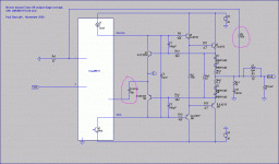
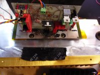
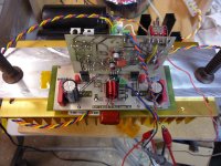
So, before seeing this and following part of Paul's suggestion, I moved the chip's feed back connection to point x on Paul's scheme and it seems to work well. I didn't move the chip's compensation cap. I'll post pictures tomorrow, all the waves looked good. I can start trying to reduce the compensation caps until oscillation sets in and then back off. Maybe this feedback strategy will allow me to remove the compensation...
I also hooked it up to the speakers and the excess brightness is gone, it sounds fantastic.
I cooked my sound card, so, no THD numbers for the moment, but, maybe in a week or two.
Ken L
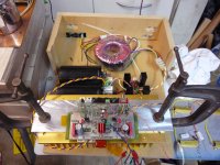
On second thought, Klewis, can you turn off any fluorescent lights? Sometimes those cause interference looking a lot like the noise on those scope shots. Also, is your scope "floating" relative to the circuit? If so, it would reduce noise if you ground your scope to the circuit's ground.
- keantoken
When I moved the Chip feedback to point x I removed the 10 ohm resistor that was tried between the emitters of the allison transistors. I can try connecting the scope at that location again to see if the noise is still present. I'll try it with the lights off. I've always made it a practice of connecting the scope's ground to the circuit's ground.
Ken L
I'm glad it's working well.
The brightness having gone away is a very good sign.
Now that I think about it, taking feedback from the Allison emitters has the same affect as driving it directly to the emitters with local feedback; it should work, and the Allison will only add a small amount of distortion.
[Judging by this experience, it seems the Allison is easier to make work when it's outside of a feedback loop; this comes as no surprise, as the Allison isn't very stable unless you dope it up on compensation]
- keantoken
Last edited:
Klewis,
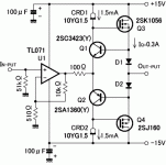
If you want to modify the Allison output stage to be a Class AB amplifier, then the attached circuit shows how. Adding two schottky diodes and reducing Re to 0.1 ohms will give a bias current of 360mA (it will start at 260mA with cold diodes). The OnSemi model for the mbr1045 and LTspice will indicate a bias current of 460mA, but it is actually 360mA.
Note the following:
- Two schottky diodes (mbr1045 or mbr745 would be good choices) and added to each Re emitter resistor. This (and Re3) is a modification to one of Kenpeters designs of some time ago.
- Re3 (33ohm) is used as a `keep alive' current to keep the output transistors, drivers and Allison bias transistors always on (and this is a good thing).
- Rf is moved to provide overall feedback, as the Schottky diodes increase the distortion such that some feedback will be required to reduce it.
- Ccomp stays on point X.
The two schottky diodes give a very smooth transition from conducting to non conducting, and hence produce less high order harmonics than normal (another good thing). If you want to model this, the OnSemi mbr1045 spice model is the closest that I could find to actual devices.
The Allison bias transistors should be thermally bonded to schottky diodes D1 and D4. Ksc3503 and Ksa1381 To126 transistors are good choices for these. Keep these diodes and Allison bias transistors away from the output device heatsinks, and ventilate well. Try to keep them at a constant temperature.
The bias current of 360mA will give Class A operation up to about 4 Watts into 4 ohms with quite low distortion. Most music is below 4 watts.
I suggest you try to get the Class A version working first, then add the Schottky diodes and Re3.
I hope this is of interest.
Paul Bysouth, Nov 2009
Attachments
Klewis,
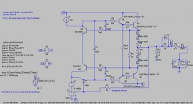
I seem to have confused you. I meant that you could try the scheme as in the attachment below. By connecting Ccomp and Rf to point X, it splits the amplifier into a front end with gain (the lme49811) and a unity gain class A output buffer. The Lme49811 provides the current source for the Allison bias and driver base currents. The Allison Class A stage has sufficiently low THD that it doesn't need overall feedback.
I have now idea what compensation the lme49811 will need, you'll have to experiment until you find the right values. The suggested values for the Allison bias are suggested starting points. 560ohm/100pF should be a reasonable starting point. Note I haven't added all the lme49811 detail, see Kenpeter's post #333 for that.
Note that this design is only suitable for a Class A amp with lots of bias current (2+ Amps).
If you want a Class AB, then a different cicruit is needed.
Paul Bysouth, Nov 2009.
Paul,
No, you didn't confuse me, I probably failed to communicate what I did. What I did was just what you drew, except, I didn't move the Chip's compensation cap (Cc), rather left is as is. I'll try moving it when I have my sound card working so that I can do a/b THD measurements.
The compensation for the allison is also as you have shown. My comment about reducing it was related to your post the other day that talked about experimenting to lower the 100pf value of the caps.
Ken
Klewis,
If you want to modify the Allison output stage to be a Class AB amplifier, then the attached circuit shows how. Adding two schottky diodes and reducing Re to 0.1 ohms will give a bias current of 360mA (it will start at 260mA with cold diodes). The OnSemi model for the mbr1045 and LTspice will indicate a bias current of 460mA, but it is actually 360mA.
Note the following:
- Two schottky diodes (mbr1045 or mbr745 would be good choices) and added to each Re emitter resistor. This (and Re3) is a modification to one of Kenpeters designs of some time ago.
- Re3 (33ohm) is used as a `keep alive' current to keep the output transistors, drivers and Allison bias transistors always on (and this is a good thing).
- Rf is moved to provide overall feedback, as the Schottky diodes increase the distortion such that some feedback will be required to reduce it.
- Ccomp stays on point X.
The two schottky diodes give a very smooth transition from conducting to non conducting, and hence produce less high order harmonics than normal (another good thing). If you want to model this, the OnSemi mbr1045 spice model is the closest that I could find to actual devices.
The Allison bias transistors should be thermally bonded to schottky diodes D1 and D4. Ksc3503 and Ksa1381 To126 transistors are good choices for these. Keep these diodes and Allison bias transistors away from the output device heatsinks, and ventilate well. Try to keep them at a constant temperature.
The bias current of 360mA will give Class A operation up to about 4 Watts into 4 ohms with quite low distortion. Most music is below 4 watts.
I suggest you try to get the Class A version working first, then add the Schottky diodes and Re3.
I hope this is of interest.
Paul Bysouth, Nov 2009
Paul,
Did you change the drawing in the last minute? I thought I just saw Rf connected to point x, now it's back with the output in the within the chip's feedback loop.
Ken
Klewis,
If you want to modify the Allison output stage to be a Class AB amplifier, then the attached circuit shows how. Adding two schottky diodes and reducing Re to 0.1 ohms will give a bias current of 360mA (it will start at 260mA with cold diodes). The OnSemi model for the mbr1045 and LTspice will indicate a bias current of 460mA, but it is actually 360mA.
Note the following:
- Two schottky diodes (mbr1045 or mbr745 would be good choices) and added to each Re emitter resistor. This (and Re3) is a modification to one of Kenpeters designs of some time ago.
- Re3 (33ohm) is used as a `keep alive' current to keep the output transistors, drivers and Allison bias transistors always on (and this is a good thing).
- Rf is moved to provide overall feedback, as the Schottky diodes increase the distortion such that some feedback will be required to reduce it.
- Ccomp stays on point X.
The two schottky diodes give a very smooth transition from conducting to non conducting, and hence produce less high order harmonics than normal (another good thing). If you want to model this, the OnSemi mbr1045 spice model is the closest that I could find to actual devices.
The Allison bias transistors should be thermally bonded to schottky diodes D1 and D4. Ksc3503 and Ksa1381 To126 transistors are good choices for these. Keep these diodes and Allison bias transistors away from the output device heatsinks, and ventilate well. Try to keep them at a constant temperature.
The bias current of 360mA will give Class A operation up to about 4 Watts into 4 ohms with quite low distortion. Most music is below 4 watts.
I suggest you try to get the Class A version working first, then add the Schottky diodes and Re3.
I hope this is of interest.
Paul Bysouth, Nov 2009
Paul,
Thanks for the schematic, yes it is quite interesting. I will give it a try. It might take a week or two for me to report back on the results. Now I see the two versions of schematics. My goof...
Thanks again to everyone for the help.
Ken
Last edited:
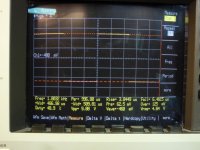
photos of square waves - I've included as the first pic the square wave output of my signal generator, you can see it has a similar shape and magnitude of overshoot to the amplified signal.
Ken L
Ken L
Attachments
The Allison bias transistors should be thermally bonded to schottky diodes D1 and D4. Keep these diodes and Allison bias transistors away from the output device
Agreed! I've already figured on my own keeping AB diodes away from outputs.
But hadn't occoured to me that bonding them to the Allison comparators might
actually be a thermal compensation worth trying!?! *Smacks forehead*
Not entirely convinced yet that cold diodes isn't the safer bet than bonded?
But certainly no harm bonding those diodes to each other if nothing else...
Unless tabs also happen to be cathodes... Then you might need a mica.
They are gonna dissipate far less than 1 Watt apiece in AB, and TO220 tabbed
Schottkys are certainly overbuilt to handle more than our application demands.
I just don't see bias runaway becoming a problem, long as they are well away
from other sources of heat...
Last edited:
Klewis,
If you want to modify the Allison output stage to be a Class AB amplifier, then the attached circuit shows how. Adding two schottky diodes and reducing Re to 0.1 ohms will give a bias current of 360mA (it will start at 260mA with cold diodes). The OnSemi model for the mbr1045 and LTspice will indicate a bias current of 460mA, but it is actually 360mA.
Note the following:
- Two schottky diodes (mbr1045 or mbr745 would be good choices) and added to each Re emitter resistor. This (and Re3) is a modification to one of Kenpeters designs of some time ago.
- Re3 (33ohm) is used as a `keep alive' current to keep the output transistors, drivers and Allison bias transistors always on (and this is a good thing).
- Rf is moved to provide overall feedback, as the Schottky diodes increase the distortion such that some feedback will be required to reduce it.
- Ccomp stays on point X.
The two schottky diodes give a very smooth transition from conducting to non conducting, and hence produce less high order harmonics than normal (another good thing). If you want to model this, the OnSemi mbr1045 spice model is the closest that I could find to actual devices.
The Allison bias transistors should be thermally bonded to schottky diodes D1 and D4. Ksc3503 and Ksa1381 To126 transistors are good choices for these. Keep these diodes and Allison bias transistors away from the output device heatsinks, and ventilate well. Try to keep them at a constant temperature.
The bias current of 360mA will give Class A operation up to about 4 Watts into 4 ohms with quite low distortion. Most music is below 4 watts.
I suggest you try to get the Class A version working first, then add the Schottky diodes and Re3.
I hope this is of interest.
Paul Bysouth, Nov 2009
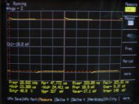
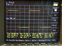
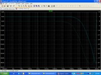
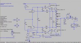
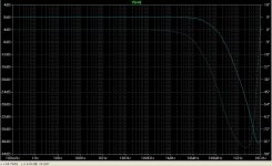
I've tried two things in simulation, first is using my original schematic without Paul's compensation of 100pf/560 ohm, but 100nf between the bases of the allison pair I get the first graph. Then with the schematic as shown, I get the second graph. Both simulate well in the four furrier analysis.
1. Is my spice schematic workable? would you change anything?
2. I was lead to believe that a phase shift over approx. 70deg was a sign of instablility. Is this correct? If so, what about the second plot?
Ken L
Attachments
Hey Kenpeter,
That page is interesting...
The circuit is interesting, wouldn't know about its performance... But the concept diagram could be done with a simple low power LTP amp, exact power needs would vary depending on the amplifier (now that I think about it this is sort of like a shunt amp).
- keantoken
That page is interesting...
The circuit is interesting, wouldn't know about its performance... But the concept diagram could be done with a simple low power LTP amp, exact power needs would vary depending on the amplifier (now that I think about it this is sort of like a shunt amp).
- keantoken
Ken,
Looking at your schematic, I think the capacitors C3 and C6 should be moved to the other side of R4, R5 - ie C6 is connected across the collector/base pins of Q8, and similarly for C3,Q9. The values of 560/100p was just a guess, so I'd try reducing the capacitor value and see how it goes.
Also try connecting one end of C2 to between the emitters of Q8,Q9 with the other end connected to R1.
Paul Bysouth
Please be specific which Ken this thread. You had me digging though my drawings...
I've come to conclusion the Caps reference to KenL's circuit, but took a while...
Thanks,
Ken P
I've come to conclusion the Caps reference to KenL's circuit, but took a while...
Thanks,
Ken P
(now that I think about it this is sort of like a shunt amp).
Yes, I see it now too. Like an Aleph turned upside down and abused as an
emitter coupled SRPP (shunt regulated push pull). I didn't see the MJK style
anti-triode totem at first, mostly due the upsidedownness and the trimpot
what multiples the emitter offset voltage to match the VAS offset...
My train of though already derailed not to see the simple EssarPeePee of it
by those misleading feedforward diagrams. Unless SRPP is a feedforward???
Edit: Nope, he blew feedforward at VR3. He's not sampling the output of
the first amp properly (directly) to compare or correct any distortions.
Flawed comparator implementation dumbs it down to SRPP. Still, not bad...
Last edited:
That site has some AMAZING stuff...
SITamp
http://www.ne.jp/asahi/evo/amp/TLB/memo0.htm
Wow, the whole chain after Q21 and Q22 seems to perform the same basic function as the Allison, except in class AB? (Q10 and Q9 are virtually Allison style, Q11 and Q12 make the difference because of their emitters' connection to output)
- keantoken
Last edited:
Yeah, but near the bottom of the page, he's finally figured out that
smooth AB don't need to be complicated. Schematic look familiar???
MOSFETs as shaping diodes IS better square law than Schottky,
but is this nuance really worth the wasted forward voltage???
And then you still gotta match them...
smooth AB don't need to be complicated. Schematic look familiar???
MOSFETs as shaping diodes IS better square law than Schottky,
but is this nuance really worth the wasted forward voltage???
And then you still gotta match them...
Attachments
Last edited:
Wow, that never even registered. Interesting he uses MOSFETs shorted G-D for the diodes...
BUT, true non-switching would be where neither OP turns completely off (or say, doesn't go below 5mA of output current). (looking at Q9, 10, 11 and 12, it looks like this is accomplished) (what if we replace Q11 and Q12 with schottkeys...?)
- keantoken
BUT, true non-switching would be where neither OP turns completely off (or say, doesn't go below 5mA of output current). (looking at Q9, 10, 11 and 12, it looks like this is accomplished) (what if we replace Q11 and Q12 with schottkeys...?)
- keantoken
Last edited:
Ken,
Looking at your schematic, I think the capacitors C3 and C6 should be moved to the other side of R4, R5 - ie C6 is connected across the collector/base pins of Q8, and similarly for C3,Q9. The values of 560/100p was just a guess, so I'd try reducing the capacitor value and see how it goes.
Also try connecting one end of C2 to between the emitters of Q8,Q9 with the other end connected to R1.
Paul Bysouth
All,
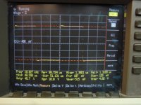
I've updated the spice schematic and messed with the values. This is the best ac analysis I'm able to get. My questions are:
Does this suggest instablity? With the exception of the diodes, it's basically the same circuit as the physical test prior to moving Rf to point x (allison emitter point) if you remember that test showed some fuzzyness at the top of the sine waves.
Is there anything else I can try?
Thanks,
Ken L
Attachments
- Home
- Amplifiers
- Solid State
- Simulation Analysis of several unique Allison-based output stages.