Keantoken,
I like your `Allison-Keane' variation to the standard Allison circuit, which overcomes the need to use large emitter resistors. However quite a bit of LTspice simulation leads be to believe that your design, and a very similar variation that I came up with, will both suffer from two problems:
- Temperature changes in the Allison bias transistors effect the output bias currents considerably and this is made worse by the small emitter resistors of the output transistors. Your design would probably benefit in using one of the THAT packages that contain 2 NPN and 2 PNP transistors. My variation was even worse.
- The transition from Class A to Class B is very abrupt, and hence will almost certainly produce high order harmonics.
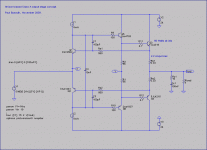
Inspired by your `Allison-Keane' design I tried to come up with a design that would allow small emitter resistors but give a gradual transition into Class B.
The attached design uses large resistors (R3, R4) to set the bias current, and then bypasses these with diodes to allow high currents without the large voltage drop across R3, R4. The diodes cause a very gradual transition into Class B, with gradual turn off, but not `Non Switching Class B style (but almost). Note that Q3,Q4 will need to be thermally bonded to D1,D2.
So far this design appears to be promising, and I hope to build and test it some time next month (my day job is getting in the way at the moment). I fear that I may have swapped one set of problems for another, namely diode switching harmonics destroying the THD figures.
I have some questions that maybe someone can answer ...
- Has anyone tried putting diodes across emitter resistors like this before, and if so, do they generate unacceptable switching harmonics?
- Is a MUR820 the best choice for the diode in this application?
Paul Bysouth, March 2009.
ps - Sorry about the delay in posting this, however my Internet router power supply decided to break just before I pressed the submit key, and as it was midnight I went to bed. I've spent this morning fixing it. I hope my cut and paste above works.
pb.
And if I subsituted BJTs for the Mosfets? And what about having utilizing Thermal Trak diodes for the output diodes?
Ken
This was taken from post #22, so, look there for the schematic.
Last edited:
Ken,
I suggest that as you currently have a Class A amplifier (and the standard Allison circuit doesn't work as an AB amplifier), that you split the amplifier into the lme49811 driver stage (with feedback), and the Allison biased Class A output stage acting as a unity gain output buffer. Don't use overall feedback! The Allison biased Class A output stage will have low enough distortion that you don't need overall feedback. This will allow you to get each half working properly, and then you can consider using overall feedback it you want to.
At the moment you have a feedback loop inside another feedback loop, and these are always difficult to track down faults. Using the `no overall feedback' scheme will help considerably
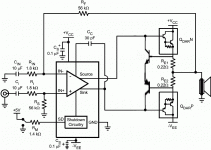
Referring to my attached output stage concept drawing, some suggestions:
1. I have looked a several loop gain control schemes, but I think the Ra1/C1 and Ra2/C2 scheme is probably the safest.
2. The resistors Ra1, Ra2 have two important functions, namely controlling the loop gain of the Allison bias circuit (in conjunction with C1, C2), and limiting excess current into the Allison bias transistors. If the output is heavily biased into Class B operation, then the voltage across the two bias transistors (Q1, Q2) will exceed 1.5 volts and so a large current will flow through Q1, Q2. These will then fail, the drivers Q5,Q6 will be pulled to the rails and Q3,Q4 will dump a large current into your speakers which will continue until either the output transistors or the voice coil fails.
3. You should have a fuse (7 Amp would be suitable) between the power supply and the output transistors, and then a capacitor from the output transistor collector to ground (eg: 1000uF plus 100nF).
4. The lme49811 has a loop gain control capacitor (C1 in your drawing I think), which is normally connected to the lme49811 sink pin. You could try moving this to point marked X on my diagram. You could also try point Y, but I think X would be better. You should also experiment with different values either side of the 10pF.
5. The feedback resistor (56 Kohm) for the lme49811 should connect to point X on my diagram.
6. If you want to implement a current limiter to stop it going into Class B operation, then 2 or 3 series diodes between point X and Vout will do the job.
I hope all this helps. I'm currently working on an Allison biased Class AB amplifier, so I'd like to see you get this working, as it may well save me some time.
It is probably time for you to update the schematic that you are using so that we can all see where you are up to.
Paul Bysouth, NOv 2009.
I suggest that as you currently have a Class A amplifier (and the standard Allison circuit doesn't work as an AB amplifier), that you split the amplifier into the lme49811 driver stage (with feedback), and the Allison biased Class A output stage acting as a unity gain output buffer. Don't use overall feedback! The Allison biased Class A output stage will have low enough distortion that you don't need overall feedback. This will allow you to get each half working properly, and then you can consider using overall feedback it you want to.
At the moment you have a feedback loop inside another feedback loop, and these are always difficult to track down faults. Using the `no overall feedback' scheme will help considerably
Referring to my attached output stage concept drawing, some suggestions:
1. I have looked a several loop gain control schemes, but I think the Ra1/C1 and Ra2/C2 scheme is probably the safest.
2. The resistors Ra1, Ra2 have two important functions, namely controlling the loop gain of the Allison bias circuit (in conjunction with C1, C2), and limiting excess current into the Allison bias transistors. If the output is heavily biased into Class B operation, then the voltage across the two bias transistors (Q1, Q2) will exceed 1.5 volts and so a large current will flow through Q1, Q2. These will then fail, the drivers Q5,Q6 will be pulled to the rails and Q3,Q4 will dump a large current into your speakers which will continue until either the output transistors or the voice coil fails.
3. You should have a fuse (7 Amp would be suitable) between the power supply and the output transistors, and then a capacitor from the output transistor collector to ground (eg: 1000uF plus 100nF).
4. The lme49811 has a loop gain control capacitor (C1 in your drawing I think), which is normally connected to the lme49811 sink pin. You could try moving this to point marked X on my diagram. You could also try point Y, but I think X would be better. You should also experiment with different values either side of the 10pF.
5. The feedback resistor (56 Kohm) for the lme49811 should connect to point X on my diagram.
6. If you want to implement a current limiter to stop it going into Class B operation, then 2 or 3 series diodes between point X and Vout will do the job.
I hope all this helps. I'm currently working on an Allison biased Class AB amplifier, so I'd like to see you get this working, as it may well save me some time.
It is probably time for you to update the schematic that you are using so that we can all see where you are up to.
Paul Bysouth, NOv 2009.
Attachments
Paul, maybe not realistic to simulate driving into emitter input impedance from 0 Ohm
signal source? If a signal source was really that low impedance, why would we need
an Allison stage??? If you sim from realistic source with 600 or 1K impedance, you find
the difficulty. AC drive signal into Q5 and Q6 bases still must come entirely from V1!
Impedance into MOSFETs works to around 22K at 20KHz. Not entirely sure with BJT
Darlingtons, but I got a sneekin feelin that input Z could appear even lower...
Its a great drawing for topology discussion, but not likely to sim meaningfully in terms
of bandwidth or distortion until this unrealistic signal source is addressed.
I like your Darlington outputs, cause we do need at least 2 emitter drops standing
on collectors Q1 and Q2. I always worried early Sziklai variants, cause there seems
barely .6V dropped across CE! Requiring those transistors flirt with deep saturation
to sustain such levels of conductivity. Can they be fast when flooded with so many
carriers? Darlington and/or enhancement MOSFET here neatly avoids that issue.
Last edited:
Klewis, what is your aim in trying out the Allison? The circuit is very adaptable and we could suggest the best mod to fit your needs.
(and yes, you could replace the output transistors with MOSFETs, BUT, bandwidth suffers.)
Yes, if you simulate with say 1k source impedance, you discover the nastiness of the Allison, you know it has to be there somewhere. The circuit's input impedance is only as linear as the output devices' Hfe curves. In this respect MOSFETs are much better. Mosfets with BJT drive overcomes bandwidth mostly.
- keantoken
Last edited:
And if I subsituted BJTs for the Mosfets? And what about having utilizing Thermal Trak diodes for the output diodes?
You want the shaping diodes NOT influenced by output transistor heat.
Schottkys have magic AB curves. And lower dropout than PN junction,
so they won't be getting hot in this application anyways....
See, the output transistors can be whatever temp they wanna be, cause
they got the Allison (or Aleph) local feedback making sure they don't go
dumping too much current into the output resistor network.
If you replace some of this resistance with shaping diodes, then you gotta
be extra concerned those diodes don't get hot and increase bias current.
This won't be a problem if you keep the diodes away from the transistors,
completely the opposite intent of Thermaltrak!!!.
In "normal" class AB outputs, those diodes are often the uncorrected
emitters of hot power transistors themselves. N curve doesn't match
the P, and rising temperature screws with both. We got it much better
with hot but "perfect"ly corrected power emitters and bias currents,
completely separate from cold Schottkys to compute the nice mating
AB curves.
Last edited:
Ken,
With the lme49811 you are actually current driving the Allison bias transistors through their collectors. I should have cut the V1 voltage source off the drawing as it is obviously confusing.
The Allison stage can be voltage driven via the emitter juntcions (ie point X on my drawing), and will work very well provided that it is a low output impedance voltage source. The Allison stage can also be current driven via the collectors, and this also works well but probably not quite as well as voltage drive. In any practical amplifier, creating a good low output impedance VAS stage probably isn't worth the trouble, while creating a current drive VAS stage is easier. Using the lme49811 to current drive the Allison bias transistors should work well.
Paul Bysouth
Current or voltage driving unknowable Z? Matters not when you got LME49811
GNF loop wrapped around, it all comes clean in the wash. Or so the theory...
Still sounds like ringing late overcorrection bait to me...
If you are gonna drive with current VAS, why you sim with perfect low Z Volt
source? You know real Z is delayed by every real and parasitic cap in the loop.
GNF loop wrapped around, it all comes clean in the wash. Or so the theory...
Still sounds like ringing late overcorrection bait to me...
If you are gonna drive with current VAS, why you sim with perfect low Z Volt
source? You know real Z is delayed by every real and parasitic cap in the loop.
Last edited:
Alright you guys, you'll let me know when you have agreed upon a direction. 😉
I like the idea of seperating the feedback loops. I already know that I can combine the sink and source from the LME49811 and the feedback - it's how I test the chip to make sure I have it set up correctly. Also the chip has a very low THD as well, as an esthetic aside it runs purly class A as well.
I infer that this means that I can't use the current from the chip and will have to use current generators for the Allison section. Is this correct?
I noticed that keantoken tried bootstrapping as well, didn't read far enough to see if that was a better approach than the current mirror. I like the bootstrapping as it has fewer parts(and less chance that I screw up the thing).
Keantoken asked about my goals... well, I was looking for other Class B bais schemes and had read this post many months ago. So, I stumbled into Class A... I've always wanted to building Class A, funny how things happen. As an aside I've built an inverting preamp around the national current feedback opamp. Very fast, very quiet, interesting project, with, I might add DC servo. Back to the goals, I'd like to be able to use my current power supply which is pretty stout at approx. 33 volts DC without making the mother of all heat sinks, so drifting into Class B seems to make some sense here. If you all say bail on the existing tranny, well, I could be talked into it. In parallel, I'm trying to make a good scheme for a Class B driven by the LME49811 with Thermal Traks.
Ken
Ken,
I suggest that as you currently have a Class A amplifier (and the standard Allison circuit doesn't work as an AB amplifier), that you split the amplifier into the lme49811 driver stage (with feedback), and the Allison biased Class A output stage acting as a unity gain output buffer. Don't use overall feedback! The Allison biased Class A output stage will have low enough distortion that you don't need overall feedback. This will allow you to get each half working properly, and then you can consider using overall feedback it you want to.
At the moment you have a feedback loop inside another feedback loop, and these are always difficult to track down faults. Using the `no overall feedback' scheme will help considerably
Referring to my attached output stage concept drawing, some suggestions:
1. I have looked a several loop gain control schemes, but I think the Ra1/C1 and Ra2/C2 scheme is probably the safest.
2. The resistors Ra1, Ra2 have two important functions, namely controlling the loop gain of the Allison bias circuit (in conjunction with C1, C2), and limiting excess current into the Allison bias transistors. If the output is heavily biased into Class B operation, then the voltage across the two bias transistors (Q1, Q2) will exceed 1.5 volts and so a large current will flow through Q1, Q2. These will then fail, the drivers Q5,Q6 will be pulled to the rails and Q3,Q4 will dump a large current into your speakers which will continue until either the output transistors or the voice coil fails.
3. You should have a fuse (7 Amp would be suitable) between the power supply and the output transistors, and then a capacitor from the output transistor collector to ground (eg: 1000uF plus 100nF).
4. The lme49811 has a loop gain control capacitor (C1 in your drawing I think), which is normally connected to the lme49811 sink pin. You could try moving this to point marked X on my diagram. You could also try point Y, but I think X would be better. You should also experiment with different values either side of the 10pF.
5. The feedback resistor (56 Kohm) for the lme49811 should connect to point X on my diagram.
6. If you want to implement a current limiter to stop it going into Class B operation, then 2 or 3 series diodes between point X and Vout will do the job.
I hope all this helps. I'm currently working on an Allison biased Class AB amplifier, so I'd like to see you get this working, as it may well save me some time.
It is probably time for you to update the schematic that you are using so that we can all see where you are up to.
Paul Bysouth, NOv 2009.
Paul,
I re-read you note for the third time - I'm a bit slow it seems. So, if I connect the Rf and cap you noted to point X and the sink and source at the appropriate current source locations, this will seperate the feedback loops - yes?
I'm less sure about how to reduce the bais to get it into Class B at a lower current - eg less heat generation. (If this makes any sense at all)
Ken
One last note the current LME49811 schematic is for a two pole compensation scheme, it can easily be changed to a single pole using a 33pf cap. I don't think it changes how the 10pf cap is connected.
Last edited:
One more question. What would the simulation model look like that had a sink and source input to the CAS?
KenL
KenL
Alright you guys, you'll let me know when you have agreed upon a direction. 😉
I like the idea of seperating the feedback loops. I already know that I can combine the sink and source from the LME49811 and the feedback - it's how I test the chip to make sure I have it set up correctly. Also the chip has a very low THD as well, as an esthetic aside it runs purly class A as well.
I infer that this means that I can't use the current from the chip and will have to use current generators for the Allison section. Is this correct?
I noticed that keantoken tried bootstrapping as well, didn't read far enough to see if that was a better approach than the current mirror. I like the bootstrapping as it has fewer parts(and less chance that I screw up the thing).
Keantoken asked about my goals... well, I was looking for other Class B bais schemes and had read this post many months ago. So, I stumbled into Class A... I've always wanted to building Class A, funny how things happen. As an aside I've built an inverting preamp around the national current feedback opamp. Very fast, very quiet, interesting project, with, I might add DC servo. Back to the goals, I'd like to be able to use my current power supply which is pretty stout at approx. 33 volts DC without making the mother of all heat sinks, so drifting into Class B seems to make some sense here. If you all say bail on the existing tranny, well, I could be talked into it. In parallel, I'm trying to make a good scheme for a Class B driven by the LME49811 with Thermal Traks.
Ken
The bootstraps work, but not as well as the current mirrors. I would only use them if you want the added simplicity (look for the most recent boostrap schematics, they have the best implementation...).
I advise to use the schottkey version if you're worried about efficiency. However, this will not be true class A, and I advise to use the pure class A Allison if you intend to call it a class A amp in the end.
The chip should give the same performance if you use it the same way you've been doing (there is nothing wrong with the current setup that I can see, though those scope shots look strange...). BUT, stability might differ (I suspect it will get better) if you connect the sink/source outputs and drive it like Paul.
You can't lower the Allison's dissipation except by using schottkeys in series with the .22 ohm resistors. Increasing the .22's will decrease bias current but this will simply cause it to clip when power is exceeded.
- keantoken
Seen those circuits that abuse a single ended opamp as-if it were differential
by grounding the output, then taking in power through current mirrors? I do
not see any easy way to make that one a Class A-able hack.... Maybe if the
chip had twin op-amps, inputs in parallel, and then you "ground" one output
of each to opposing rails... I dunno if that could actually work or not?
Heywaitaminute... What happened to discrete components?
I was just checking the LME49811 to see exactly what kinda op-amp
it is you been trying to use so far. Looks appropriate without having
to do any such stupid abuse as I was thinking...
Allison (sliding bias correction only, no other errors corrected except
by the op-amp) seems a no-brainer. So, whats been the trouble???
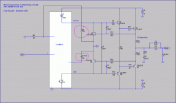
Copy and paste National's reference design...
Then the Allison hack...
it is you been trying to use so far. Looks appropriate without having
to do any such stupid abuse as I was thinking...
Allison (sliding bias correction only, no other errors corrected except
by the op-amp) seems a no-brainer. So, whats been the trouble???
Copy and paste National's reference design...
Then the Allison hack...
Attachments

Last edited:
The trouble is that that Allison is unstable without compensation, and Klewis had no difficulties discovering that! 🙂
However, there are some odd bumps on those scope shots, and the noise looks like it is aperiodic oscillation of the Allison. We're having problems primarily with the Allison, not with the chip, which is holding up stoically.
Klewis, it should help if you increase the stability compensation of the 49811 to much higher than its current value, then we'll be more sure it's not the chip causing problems, and it should be easier to troubleshoot. After things are working, then why not find the optimal compensation values?
- keantoken
On second thought, Klewis, can you turn off any fluorescent lights? Sometimes those cause interference looking a lot like the noise on those scope shots. Also, is your scope "floating" relative to the circuit? If so, it would reduce noise if you ground your scope to the circuit's ground.
- keantoken
- keantoken
Klewis, is it possible that you were slightly overdriving the Allison when you saw the bump in the picture? That is the only explanation I know of...
- keantoken
- keantoken
I don't see how Cc (the bootstrap?) in ref design is supposed work
off the current "sink" only, if its really a single ended class A???...
You need to tie that bootstrap to the output of the Allison, where
that end of the cap can be brutally jerked equally in both directions.
off the current "sink" only, if its really a single ended class A???...
You need to tie that bootstrap to the output of the Allison, where
that end of the cap can be brutally jerked equally in both directions.
Okay, I looked back and didn't find my aforesaid "bootstrap schematic".
So here it is, this is how it's done. This works better than taking bootstrap reference straight from the output.
Ken, you may have seen a speculative schematic for an RF-themed Allison variant.
- keantoken
So here it is, this is how it's done. This works better than taking bootstrap reference straight from the output.
Ken, you may have seen a speculative schematic for an RF-themed Allison variant.
- keantoken
Attachments

Last edited:
Klewis,
I seem to have confused you. I meant that you could try the scheme as in the attachment below. By connecting Ccomp and Rf to point X, it splits the amplifier into a front end with gain (the lme49811) and a unity gain class A output buffer. The Lme49811 provides the current source for the Allison bias and driver base currents. The Allison Class A stage has sufficiently low THD that it doesn't need overall feedback.
I have now idea what compensation the lme49811 will need, you'll have to experiment until you find the right values. The suggested values for the Allison bias are suggested starting points. 560ohm/100pF should be a reasonable starting point. Note I haven't added all the lme49811 detail, see Kenpeter's post #333 for that.
Note that this design is only suitable for a Class A amp with lots of bias current (2+ Amps).
If you want a Class AB, then a different cicruit is needed.
Paul Bysouth, Nov 2009.
Attachments
- Home
- Amplifiers
- Solid State
- Simulation Analysis of several unique Allison-based output stages.