Hi All,
How about a mono block good for 20W to 1KW+ based on SiLabs ISO drivers with a few nifty features and a considerable mod/DIY appeal?
Context
I’ve been lurking a lot around here lately, studying various class-d designs being proposed, discussed and implemented. Back in may this year, somebody asked about a silicon labs driver ic and whether it would be a good alternative to the various IRS designs.
Here is the relevant web page. Having been familiar with Silicon Labs microcontrollers for a longtime (my job is analog/digital/RF/firmware design, DISCLAIMER: I am in no way involved with Silabs), I became aware of their class D drivers last year when they were first presented. Neat chip I thought, simple, well designed and with a few good features: isolated; precisely settable dead time down to a couple nanoseconds; comes in two driving strengths (0.5A for up to 400W and 4A for higher output designs); supports supply rails up to +/-750V (if that tickles your fancy). I liked the fact that they left out the error amp and modulator.
Other specs sounded good, and at that point I wondered how an amp based on the chip would sound in the real world. I also wondered why it hadn’t caught any traction in the DIY community. Maybe the manufacturer just isn’t known enough outside the microcontroller or RF space. Also, DIY’ers aren’t particularly attracted to SMD packages, and the Silicon Labs drivers do not come in DIP.
Silicon Labs do offer a reference design (RD), the Si824xClassD-KIT, delivering 2x 120W into 8 Ohms, for 299 USD (Mouser). After reading its user’s guide, I decided the board wasn’t for me. Not for use as one of my amps anyway. Reasons: a) form factor b) the protection circuitry and logic is a bit cluttered IMO c) last but not least, its price.
The plan
So, long story short, I started designing my own. Actually I’m still in the process, but would like to get early feedback and comments before committing to it, then fabbing and stuffing a few PCBs for myself and anyone else here interested in trying out the design, possibly with different configurations.
The highlights
- Mono block, BTL, uses two Si824x chips
- single supply from 12 to maybe 100V
- supports a separate 12V supply for gate drivers and input/logic
- undervoltage lockout, (over)current sensing for each arm
- heatsink temperature sensing, plus true wattmeter on output
- protection circuitry calibration, logic and UI on daughterboard
- daughterboard possibly uses microcontroller for shutdown logic and more
- mostly SMD, some TH components for easier adapting/experimenting
Form Factor
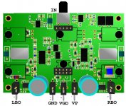
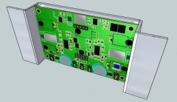
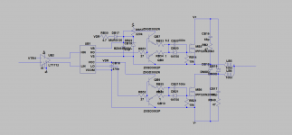
For starters, here is the form factor I came up with so far. (No routing yet, I’d like to stay some more time in the placement phase). Measuring 90 by 60mm, it fits onto a heatsink plate or extruded profile. Output MOSFETs are TO-220, mounted underneath the board which has holes drilled to access the mounting screws for the transistors.
http://www.diyaudio.com/forums/attachment.php?attachmentid=237851&stc=1&d=1314661880
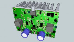
Two TO-220 BJTs are mounted in the same way. One is the regulator for the gate drive voltage, and the other is a Vbe temperature sensor.
Input is at the top of the board via an RCA jack, while output and power connections are at the bottom. These can be either screw terminal blocks, or faston males.
Below are two possible heatsink mounting options, the first could be built into a (low power) active speaker, the second is beefier.
http://www.diyaudio.com/forums/attachment.php?attachmentid=237854&stc=1&d=1314661880
Of course, many more variations are feasible. BTW can you tell I have been fighting with Sketchup?
http://www.diyaudio.com/forums/attachment.php?attachmentid=237855&stc=1&d=1314661880
The two metal cubes are the output inductors. The layout accomodates the SAGAMI as in the RD, the Wurth WE-PD, plus there is enough real estate to accomodate larger toroids.
Architecture
The idea is to keep the signal path very much in line with the Silabs reference design, while re-inventing the protection circuitry and logic wheels, and adding a few niceties here and there. I'll post and go through the schematics right after this. I went for SMD mostly because I am familiar with it, but am leaving several key components as through hole. Apart from the power MOSFETs, “key” means that the component value will likely have to change with different power supply / output levels, or, as in the case of the dead time setting resistors, will depend on the chosen MOSFETs and will have to be experimented with.
The result is a ucd (self-clocking), mono block in BTL configuration able to pump 1KW and more depending on its single supply rail (and the choice of MOSFETs, and...). For myself here at home, I’d be happy with two channels with 50W into 4Ohms, using a lowly 24V/3A SMPS, or two 12V batteries. Later perhaps a third, with higher power, to drive a subwoofer.
Ok, I’ll post the schematics in a bit, or rather tomorrow, it’s getting late. Thanks for reading.


