I find that flooding the scrubbed board with a big splash of alcohol, wiping/drying vigorously with a crumpled pad of 3 kleenex tissues, and then immediately blasting the PCB with a hair dryer, gets rid of most of the haze. 1 second with the tissues, drop them on floor and grab already-plugged-in hairdryer (elapsed time: 0.5 seconds), dry for 10 seconds. Modulate the hot air/cold air switch as needed to avoid burnt fingertips. Wear gloves if skin is sensitive to highly concentrated alcohol.
Thanks Mark.
I have too many questions...sorry.
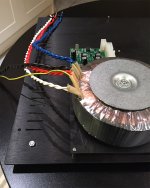
Jumping ahead a little, attached is a pic of my transformer sitting on its mounting plate which is in turn attached to the enclosure bottom. (I will likely flip the transformer up the other way so the leads point downwards.) I asked for it to be supplied with extra long leads. I need to connect the transformer at the front of the enclosure to the soft start board which is attached to the rear panel of the enclosure. Is it better practice to cut the primary leads short and do the run across the enclosure base with a heavily shielded mains cable or does it not really matter and hence I should just use the white primary wires from the transformer for the run? I'm wondering how to minimise EMI within the enclosure.
I have some 300V, 14AWG shielded mains cable (used for power cords) that I can use. Its shield is attached to a wire that can be grounded (which would, I believe, create a Faraday shield).
Also, as previously discussed the transformer shield needs to be grounded. A somewhat convenient place is the chassis ground point - again across the enclosure on the rear panel. If I use the mains cable for the run across the enclosure I can use its earth wire to connect the transformer shield to the chassis ground point. If I don't use the mains cable run and just use the existing transformer wires, is there any best practice, e.g. twisting the shield ground wire with the primaries, for running this wire?
I have too many questions...sorry.
Jumping ahead a little, attached is a pic of my transformer sitting on its mounting plate which is in turn attached to the enclosure bottom. (I will likely flip the transformer up the other way so the leads point downwards.) I asked for it to be supplied with extra long leads. I need to connect the transformer at the front of the enclosure to the soft start board which is attached to the rear panel of the enclosure. Is it better practice to cut the primary leads short and do the run across the enclosure base with a heavily shielded mains cable or does it not really matter and hence I should just use the white primary wires from the transformer for the run? I'm wondering how to minimise EMI within the enclosure.
I have some 300V, 14AWG shielded mains cable (used for power cords) that I can use. Its shield is attached to a wire that can be grounded (which would, I believe, create a Faraday shield).
Also, as previously discussed the transformer shield needs to be grounded. A somewhat convenient place is the chassis ground point - again across the enclosure on the rear panel. If I use the mains cable for the run across the enclosure I can use its earth wire to connect the transformer shield to the chassis ground point. If I don't use the mains cable run and just use the existing transformer wires, is there any best practice, e.g. twisting the shield ground wire with the primaries, for running this wire?
Attachments
Last edited:
Scotsmen don't need gloves, they are all insensitive to strong alcohol.................. Wear gloves if skin is sensitive to highly concentrated alcohol.
That's why our National Health Service has to spend so much of our money on treating injuries related to alcohol consumption.
Smoke
I take it that smoke is never a good sign in electronics....
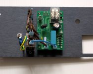
I connected up the soft start, added the transformer and measured secondary voltages. The 17V nominal secondary read 18.4V. I then proceeded to connect the 12V regulator module. The only load was my multimeter.
A wisp of smoke (and I wasn't getting 12V out) and that 'oh no' smell. In terms of obvious damage, R6 is definitely toast. Nothing else obvious. Of course, R6 is about the most difficult to reach part (lesson for the future).
In terms of trouble shooting this is there anything I should be doing other than replacing R6 and having another go? (I'd prefer not to make things worse.)
I take it that smoke is never a good sign in electronics....
I connected up the soft start, added the transformer and measured secondary voltages. The 17V nominal secondary read 18.4V. I then proceeded to connect the 12V regulator module. The only load was my multimeter.
A wisp of smoke (and I wasn't getting 12V out) and that 'oh no' smell. In terms of obvious damage, R6 is definitely toast. Nothing else obvious. Of course, R6 is about the most difficult to reach part (lesson for the future).
In terms of trouble shooting this is there anything I should be doing other than replacing R6 and having another go? (I'd prefer not to make things worse.)
Attachments
Last edited:
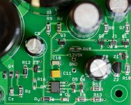
Is there any chance that the test hardware was mis-configured? Did a zero-ohm R15 short R6 to the +12VIN port, which explains the burnout? Is zener diode Z1 also destroyed?
Is C6 to blame for R6's demise? Is C6 shorted? Is it installed backwards?
Is the opamp to blame for R6's demise? It appears to me that removing the opamp from its socket won't do anything bad except cease regulating and let Vout rise up to (Vin - Vth_q4). After replacing R6 you could gingerly power-up with the opamp removed from its socket.
Speaking of gingerly power-up operations, do you own a Variac? (Amazon UK example) Mine has saved me from explosive disasters more than once.

I've still not had time to do the full 'chop chop box' tests but I did have time to run the 12V PSU for a bit with a constant load - first 8 Ohms/1.5A for 15 minutes or so, then 4 Ohms/3A for about 10 minutes and finally 4R and 8R in parallel for 4.5A for a further 5 minutes or so. Much longer than that and the load resistors would have been getting extremely hot.
All appeared fine. What I did notice, however, was that with 3A and above my transformer began to buzz. I had the mains lead connected directly into the socket. Is this 'DC on the mains'?
All appeared fine. What I did notice, however, was that with 3A and above my transformer began to buzz. I had the mains lead connected directly into the socket. Is this 'DC on the mains'?
If you own an isolation transformer or a powerline conditioner which includes a transformer, you can exploit the fact that it also blocks DC. Plug it in upstream of your new 12V PSU with 3.5A load and see whether the buzz disappears.
If you don't own an isolation transformer, you may decide you would prefer to spend your money and your time constructing a bridge-plus-caps DC blocker. I myself am drawn to Figure 8 of Rod Elliott's design, but I haven't actually built one. You can get a 35 ampere bridge rectifier for less that 4 USD, and the capacitors are cheap too:
Or you may decide you would prefer to spend your money on an isolation transformer. If you do I recommend getting the biggest VA rating you can afford (including shipping). Online auction sites like eBay might be the place to look first.
If you're worried about capacitors rated for "only" 6.3 volts, remember that the two series 35A diodes clamp the capacitor voltage to 2.0 volts or less. If you need additional reassurance look at the DC blockers built inside the large Bryston amplifiers (schematics download page) -- you'll see that they use 6.3VDC rated caps too.
I don't think that an isolation transformer does that.
The DC effect is not due to DC superimposed on the AC waveform.
It is due to asymmetrical waveform where the area above the zero volts line and the area below the zero volts line are not equal.
This can be due to harmonics of the mains frequency that are applied in an asymmetrical manner, eg. 2nd creates an upper to lower waveform difference.
A big EI isolation transformer will not pass all the harmonics. This may improve the symmetry of the waveform, particularly if it's the VHF harmonics that are creating the non symmetrical waveform.
This is effectively a filtering effect.
The capacitor form of DC blocker seems to be a more effective filter of the asymmetry in the waveform.
Last edited:
the noise could be the pulses of current stimulating a vibration of loose wires/laminations inside the transformer.I've still not had time to do the full 'chop chop box' tests but I did have time to run the 12V PSU for a bit with a constant load - first 8 Ohms/1.5A for 15 minutes or so, then 4 Ohms/3A for about 10 minutes and finally 4R and 8R in parallel for 4.5A for a further 5 minutes or so. Much longer than that and the load resistors would have been getting extremely hot.
All appeared fine. What I did notice, however, was that with 3A and above my transformer began to buzz. I had the mains lead connected directly into the socket. Is this 'DC on the mains'?
The rectified and smoothed output imposes short high current pulses in both the primary and the secondary of a mains transformer.
It is these high current pulses that require a transformer to be down rated from simple resistor loading specified rating to rectified & smoothing rating.
The POWER available as a DC supply/current is roughly 70% of the rated VA of the transformer. This is to keep the I²R losses low enough to not overheat the windings. The DC CURRENT available is roughly half the rated AC current of the transformer.
If you are drawing 4.5A of DC current, that is the equivalent heating effect to using a 9Aac rated winding at maximum power. How close is 9Aac to your specified AC rating?.
I'm still trying to digest Andrew's posts. In the interim, here are some details of the transformer:
- custom "audio grade" toroid from Toroidy
"Audio grade transformer is dedicated for use in power amplifiers and other high-end audio devices. In audio grade, noiseless transformer price You'll get transformer wound on high inductive, selected and measured core. Core and all the windings will are impregnated. Transformer will also has electric and electromagnetic shields, epoxy filled interior and mounting pads in price." sic
- 350VA
- primary 230V
- secondaries: 10A@17V, 10A@8V and 10A@7V
Andrew, are you saying I didn't size it large enough? I took my PSU DC 'spec' of 5A and doubled it for each secondary which seems in line with your guidance (to not overheat the windings) or do I not have enough headroom?
Last edited:
Naah, you're good. For the 12V supply you're pulling 5A from (17 x sqrt(2)) volts {conservatively assuming zero ripple!} which is 120.2 watts. The secondary is rated for 170VA. Plenty of safety margin.
Or you can do what I did: either buy a DMM that ships with a thermocouple (like this one) or else buy an infrared thermometer (like that one).
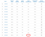
Measure the temperature of the ambient air. Then turn on your power supply with full load on +12V and measure & record the transformer temperature every 2 minutes for 30 minutes. {a smartphone set to "stopwatch" mode helps, so does an egg timer}.
Now you have sixteen datapoints (time_since_turnon, transformer_temperature). Plot them on an XY curve. What is the final asymptote at time=Infinity? What is the "temperature rise"? Rise = (Final_Toroid_Temperature - Ambient_Air_Temperature)
Budget yourself 50 degrees Celsius or less of "temperature rise" for the transformer as a whole. 50C is pretty typical of transformer manufacturer specs, see below. For the 12VDC output {the 17VAC winding} you get (17x10) / ( (17x10) + (8x10) + (7x10) ) = 170/320 = 53.1% of the budget. When you're only loading the 17VAC winding, the "temperature rise" should be less than 26.5 degrees C, extrapolated out to time=infinity.
You may find that a curve fitting program shows an excellent match between your datapoints and a textbook classical exponential rise:
_
Or you can do what I did: either buy a DMM that ships with a thermocouple (like this one) or else buy an infrared thermometer (like that one).
Measure the temperature of the ambient air. Then turn on your power supply with full load on +12V and measure & record the transformer temperature every 2 minutes for 30 minutes. {a smartphone set to "stopwatch" mode helps, so does an egg timer}.
Now you have sixteen datapoints (time_since_turnon, transformer_temperature). Plot them on an XY curve. What is the final asymptote at time=Infinity? What is the "temperature rise"? Rise = (Final_Toroid_Temperature - Ambient_Air_Temperature)
Budget yourself 50 degrees Celsius or less of "temperature rise" for the transformer as a whole. 50C is pretty typical of transformer manufacturer specs, see below. For the 12VDC output {the 17VAC winding} you get (17x10) / ( (17x10) + (8x10) + (7x10) ) = 170/320 = 53.1% of the budget. When you're only loading the 17VAC winding, the "temperature rise" should be less than 26.5 degrees C, extrapolated out to time=infinity.
You may find that a curve fitting program shows an excellent match between your datapoints and a textbook classical exponential rise:
- Temp = Ambient + D(1 - exp(-time/tau))
_
Attachments
Thanks guys.
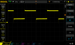
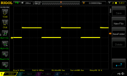
I connected the chop chop box with an 8 Ohm load and zero pre-load i.e. an easy 1.5A soft test. I'm wondering if this is what you meant previously. The gate voltage should fall to zero but doesn't appear to do so. With the load disconnected (second pic) it is fine. (Oops, note the different scales between the two pics.)
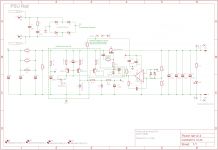
Does it manage not to thwack its own GND when delivering amperes of kaboom to its output?
I connected the chop chop box with an 8 Ohm load and zero pre-load i.e. an easy 1.5A soft test. I'm wondering if this is what you meant previously. The gate voltage should fall to zero but doesn't appear to do so. With the load disconnected (second pic) it is fine. (Oops, note the different scales between the two pics.)
Attachments
Last edited:
It looks like there is a 3.5 volt difference between (i) the place where your scope probe touches the gate node; (ii) the place where your scope ground-clip connects to the grounding network. Furthermore that voltage difference appears not to change versus time; if it were an (L/R) timeconstant, (L/R) would have to be much MICH greater than 400 microseconds -- otherwise we'd see some slope on the logic-low.
Since Iout is 1.5 amperes and deltaV = 3.5 volts, we know there exists 2.3 ohms of resistance between the MOSFET source and the scope ground clip. If the ground clip is at the power supply input terminal "J2", this means that (RX + RZ) = 2.3 ohms in the picture below. You can leave the ground clip where it is and go probing along the ground network to find where the ground voltage drops are occurring.
Oh and if (L/R) >> 400usec when R = 2.3 ohms, it means that L >> 170 microhenries. Which is crazy; your wiring inductance will be between zero and 99 nanohenries (a factor of 1000 smaller). So it's definitely a resistive voltage drop, not an inductive voltage drop.
_
Attachments
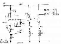
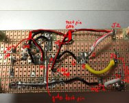
While I chew on the above*, here's a pic of my rather awful GND wiring on the actual box. Not dissimilar from your sketch, the GND connections re the LMC555 come together at one point, likewise for the MCP1407 and its filter caps which is also where I have placed the GND test pin. These are connected together. I then bring the latter to your J2 and the source of the MOSFET to J2 also.
The test pin for the gate is at the MCP1407 (pins 6 and 7).
* I'm not following. The high voltage is right at 12V. The gate's just not going to zero when low (when a load is connected).
The test pin for the gate is at the MCP1407 (pins 6 and 7).
* I'm not following. The high voltage is right at 12V. The gate's just not going to zero when low (when a load is connected).
Attachments
Last edited:
Since Iout is 1.5 amperes and deltaV = 3.5 volts, we know there exists 2.3 ohms of resistance between the MOSFET source and the scope ground clip. If the ground clip is at the power supply input terminal "J2", this means that (RX + RZ) = 2.3 ohms in the picture below. You can leave the ground clip where it is and go probing along the ground network to find where the ground voltage drops are occurring.
I'm struggling with this. I must be missing something basic in the following.
I am measuring the voltage potential between the junctions of pins 6 and 7 of the MCP1407 (which connect to the gate of the MOSFET) and where my alligator clip connects to GND (the confluence where I have joined pins 4 and 5 of the MCP1407 and the GND pins of the filter capacitors to the rest of the GND wires).
The LMC555 and MCP1407 have a rather simple job - charge and discharge the gate capacitance of the MOSFET. They charge it to the supply voltage and discharge it to GND. They (ought to) do this with 50% duty cycle regardless of the load attached and regardless of the current flowing through the heavy wires from supply to drain to source to GND (albeit, of course, the level of charge in the gate capacitance dictates how much current can flow).
The discharge path for the gate capacitance is via that where you have included RY. The chop chop box does all this dutifully when there is no load attached. If there were significant resistance RY then presumably we'd see the behaviour depicted in my left pic when no load is present, but we don't (chart on the right).
So when there's no load it can discharge G but can't do so fully when a load is attached. When a load is attached G remains 3.5V above the voltage at my GND test pin. I'm confused but will do some probing...
Last edited:
- Status
- This old topic is closed. If you want to reopen this topic, contact a moderator using the "Report Post" button.
- Home
- Amplifiers
- Power Supplies
- Adventures with 5A regulated voltage circuits