BTW I'm still surprised that I get rather different snubber measurements than your Quasimodo examples. The transformer I have is a 350VA, 230V primary with 3 secondary pairs of 17V, 8V and 7V. For the snubber resistors I get 16.2 Ohms, 13 Ohms and 13 Ohms respectively. (Through-hole Quasimodo with dipswitch pins 1 and 2 set to on for c100Hz duty cycle and Cx=10nF and Cs=150nF.)
Quasimodo gives you the chance to see the snubber actually working, with your own eyes. Just pull the trimmer out of its socket and voila, a before-and-after picture on your very own scope, using your very own transformer, viewed with your very own eyes.
However if that is not sufficient, you can always supplement the eyeballs-only, no-math approach with a math-based approach. Post #620 in the Quasimodo thread says more.
Remember that the only thing which prevents you from using an all-math approach like Hagerman's, is a single piece of data: he needs the numerical value of transformer leakage inductance. Quasimodo can help you measure this inductance. (You don't need to measure and you don't need to know transformer capacitance because Cx swamps it out as explained on p.5)
I think the very first thing you should do is look up the capacitance of your rectifier diodes, at Vfwd=0. This is found in the vendor supplied SPICE models, the parameter is named "Cjo" (Capacitance of junction at zero bias). For example the MURS320 diode model which is presupplied in LTSPICE, has a Cjo parameter value of 135 picofarads. Double check this in your LTSPICE installation and verify that your MURS320 does indeed have Cjo=135p. If so it means you are looking at the correct parameter.
What is the capacitance of the rectifier diodes you will use with this 3-secondary transformer?
Last edited:
Indeed, with Quasimodo I can see the before and after clearly, and even see the change in real time as I dial the variable resistor when my Rigol scope is set to Auto.
I will take a look at the pdf/mathematics again.
Regarding Cjo, the rectifier diodes I have purchased are the Fairchild 30A 200V FFPF30UP20STU. I could not find a Spice model for these specific diodes but Fairchild provides a model for the 20A 400V version and this is what I am using in my Spice modelling. Cjo = 8.435E-10 in their model for the FFPF20UP40S. Full Fairchild model below:
**************** Power Diode Electrical Parameters ********************
** Product: FFPF20UP40S
** Package: TO-220F-2L
* -------------------------------------------------------------------
.MODEL FFPF20UP40S D
+ IS=1.4309E-11 N=1.0 RS=0.01102 TRS1=1.5e-4
+ TRS2=1.6e-6 ISR=5.052E-9 NR=2.0 CJO=8.435E-10
+ VJ=0.6905 M=0.415 BV=440 IBV=1.0E-4
+ TT=1.1642E-8 EG=1.12
* -------------------------------------------------------------------
* Creation: May-28-2014 Rev: 0.0
* Fairchild Semiconductor
The next thing to do is to estimate the capacitance of your entire rectifier assembly, viewed from the transformer secondary. The Quasimodo design note calls this "Crectifier" on page 5.
If the rectifier assembly is a 4 diode bridge, then (the following will infuriate and enrage circuit theorists...) a pragmatic way to create a conservative overestimate of Crectifier is:
Now read page 5 of the Quasimodo design note and use Crectifier to calculate a value for Cx, the first capacitor in the CRC snubber.
If the rectifier assembly is a 4 diode bridge, then (the following will infuriate and enrage circuit theorists...) a pragmatic way to create a conservative overestimate of Crectifier is:
At the instant of diode switch-off (when oscillatory ringing is triggered), assume two of the four diodes have Vfwd=zero and assume the other two of the four diodes have Vfwd=BigNegativeNumber (the secondary peak voltage). Assume the diodes at Vfwd=0 have capacitance=Cjo, by definition. Assume the two diodes at Vfwd=BigNegative have capacitance=(Cjo/100). Assume the capacitance of the entire assembly, viewed from the transformer secondary, is the parallel combination of these capacitances. Thus Crectifier = 2.02*Cjo.
Since your best guess of your diode's Cjo is 844 picofarads, your estimate of Crectifier is 1.70 nanofarads or less {since 2.02x is a conservative overestimate}.Now read page 5 of the Quasimodo design note and use Crectifier to calculate a value for Cx, the first capacitor in the CRC snubber.
to calculate a value for Cx
I had planned to simply use 10n for Cx and 150n for Cs, i.e. the same size capacitors as included in your Quasimodo kit and in accordance with the guidance provided on pg 7 of the Quasimodo design note, and adjust Rs as necessary. Are you suggesting that, in my case, Cx should really be higher? (so as to make Crectifier and CT irrelevant)
Last edited:
your MURS320 does indeed have Cjo=135p.
big difference between these numbers. more than 6times !Cjo = 8.435E-10 in their model for the FFPF20UP40S.
I am suggesting that the component values mentioned "... at least as a starting point for further experimentation" are merely a starting point. People who begin their experiments at this starting point, only to discover they don't like the Rs value which results, are free to experiment with other values. Different transformers have different parasitic inductances and capacitances, so it's not a huge surprise when different snubber values arise.Are you suggesting that, in my case, Cx should really be {some other value} ?
Those handy with algebra will be able to look at the equations and deduce whether increasing Cx should increase, or decrease, Rs. Those not good with algebra can try both options on a real Quasimodo and find out which one gives the more desirable Rs result.
Perhaps you may find there is another value of Cx which gives a snubber resistance Rs that you like better. I think it preferable to use the reasoning on p.5 to choose a Cx, but others (notably Morgan Jones and Jim Hagerman) do not. So use your own best engineering judgment to select whichever snubber you like the most / hate the least.
Quasimodo design note appendix D. My new transformer doesn't appear to have any polarity markings. (Rather unhelpfully, both primary cables are white, both 12V red, both 8V black and both 7V blue.)
I don't have a function generator. However, can I use Quasimodo as a function generator albeit perhaps I have to look more closely at the waveform? (With dipswitch settings 1 and 2 "on" I believe it produces a 97Hz 50% duty cycle. With C3=150n in place one can gets a slop to the rise in the generated waveform.)
I tried this but I must be doing something wrong. Of course it is easy to get a clear signal for the driving waveform by placing scope channel 1 onto a pin in the C2 socket of the Quasimodo. I can send this waveform down one of the primaries by connecting it into Quasimodo's P7. However I am struggling to get a locked waveform when scope channel 2 is connected to a transformer secondary.
The high capacitance diode is rated for 6.6 times the current of the low capacitance diode. 20 amperes versus 3 amperes.big difference between these numbers. more than 6times !
Scan down the list of presupplied diodes in LTSPICE; some are 0.5 picofarads and others are 2000 picofarads. Go grab a SPICE model of a brand new 2014-model diode that's intended for solar power applications, ultra high current at ultra low Vfwd, but not very big reverse voltage rating. You'll see some truly enormous Cjo values.
Perhaps you may find there is another value of Cx which gives a snubber resistance Rs that you like better.
I don't care so much about the absolute value of Rs. I'm merely surprised that with all the transformers I have measured (a universe of 3 or so) I get materially smaller optimised values for Rs than your examples. If they're right then that's ok.
An excellent thread with some excellent references (post 6) and examples (post 11)
http://www.diyaudio.com/forums/equipment-tools/272068-chop-chop-box.html
Notice the metal heatsink inside the insulating chassis (!)
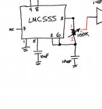
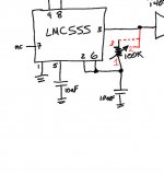
I think it would be useful to include two pins with your previously proposed test circuit (LMC555 driving an MCP1407 driving the gate of a STP27N3LH5) so that a channel of my scope can be used to monitor and trigger from the signal driving the gate of the STP FET. I notice that Elvee includes these also, labelled as "Sync". However, I was thinking of merely adding a pin connected to the gate of the FET (and of course one connected to GND). While I am still trying to understand the intricacies of his circuit (I can see the core of its operation but need to learn about hex Schmitt triggers) I note he has a 4K7 resistor R9 between the circuit and the sync pin. I don't understand why. Is my strategy of merely monitoring, directly, the gate of the STP FET flawed?
I note also your quick circuit sketch has filtering of the supply (I was planning to use a 1K resistor and 470u Nichicon cap which I have in my box) for the LMC555 but not for the MCP1407. Intentional?
(I guess if the test jig is to be powered from the DUT one of which is 3V3 then there's not a lot of voltage headroom - we've discussed 3V3 versus the indicated min supply of 4.5V for the MCP1407.)
Yet another dumb question: do I have the (physical) wiring of this potentiometer correct? The lack of connection from the wiper in circuit diagrams is confusing.
Also, I see that if one were to want to display the scale for the frequency that a logarithmic pot may be more appropriate but given I won't be doing this (unlike Elvee's example) I simply chose a linear POT. Shortsighted?
Also, I see that if one were to want to display the scale for the frequency that a logarithmic pot may be more appropriate but given I won't be doing this (unlike Elvee's example) I simply chose a linear POT. Shortsighted?
Attachments
On reflection and further investigation... I understand that making the red dotted connection is also best practice. Learning painfully slowly. PSU and remaining test jig parts arriving tomorrow. I will hopefully get the chance to complete the jig but soldering the PSU rails will have to wait until I get back from a two week family vacation.
Attachments
Last edited:

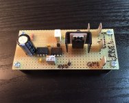
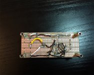
For some reason, for me the soldering was a pain in the proverbial.
I have only tested it to the extent of connecting a 9V battery and observing the waveform delivered to the gate of the Mosfet pass transistor. Initially it wasn't working but I found the bad solder joint. I get a nice square wave which varies in frequency when I turn the potentiometer. That was with no load attached.
I have only tested it to the extent of connecting a 9V battery and observing the waveform delivered to the gate of the Mosfet pass transistor. Initially it wasn't working but I found the bad solder joint. I get a nice square wave which varies in frequency when I turn the potentiometer. That was with no load attached.
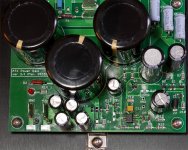
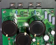
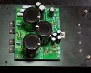
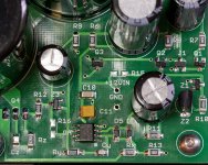
A few pics of the assembled 12V rail (Zobel at gate, Cz and Rz, rather than gatestopper resistor for now, R12). The SOD-323 diodes scared the hell out of me when I took them out of the package - tiny! - but it's interesting as were I to do the board again I would compact the SMT area of the board significantly.
I wish I could find a way to clean the pcbs a bit better. I am using Isopropyl Alcohol and a toothbrush.
I wish I could find a way to clean the pcbs a bit better. I am using Isopropyl Alcohol and a toothbrush.
Attachments
- Status
- This old topic is closed. If you want to reopen this topic, contact a moderator using the "Report Post" button.
- Home
- Amplifiers
- Power Supplies
- Adventures with 5A regulated voltage circuits