Almost every OP will oscillate if you give them a chance ")
It is more important to use proper topology/circuit and compensation than any particular OP.
By my option, SGK's voltage follower stage is not a best choice and probably it is the root cause of problems.
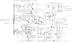
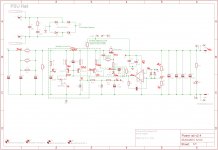
Take an look on attached PDF which show several different output stages:
1) standard positive LDO
2) as 1 but with inverted control
3) as 1 but with additional current limiter
4) as 2 but with additional current limiter
5) similar to 1 but with darlington
6) standard negative LDO (same rules apply as above)
7) high speed LDO with PMOS-FET
8) high speed LDO with PMOS-FET but with inverted control
It is more important to use proper topology/circuit and compensation than any particular OP.
By my option, SGK's voltage follower stage is not a best choice and probably it is the root cause of problems.
Take an look on attached PDF which show several different output stages:
1) standard positive LDO
2) as 1 but with inverted control
3) as 1 but with additional current limiter
4) as 2 but with additional current limiter
5) similar to 1 but with darlington
6) standard negative LDO (same rules apply as above)
7) high speed LDO with PMOS-FET
8) high speed LDO with PMOS-FET but with inverted control
Attachments
Sorry I deleted my previous post as I realised I did not have the same resolution in the pics. Here they are again: pic 1 is Vref measured at R11 and pic 2 is V+ to the op amp measured at my unused 12V+ Vin connection i.e. essentially C10 (remember jumper R15 is not populated on the 12V board).
Attachments
It is in our interest to keep reference device on "quite place", means no dinamic load on it, high input impedance of following stage even to keep them on stabile temperature.
Also I see that you trust LTSpice too much.
Simulator is good as much as you provide them more realistic models of every involved component inluding paracitic elements of PCB traces.
Your regulator have GBWP of about 10MHz (tried you ASC file), thats looks nice in simulator but in reality, huh, very big chalenge ...
Last edited:
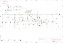
To be honest, I never seen such implementation … OUT from OP trough precise reference to GATE
Why you didn't change reference voltage on +IN of OP, or change FB divider at -IN of OP?
This just steps the voltage at the gate of the MOSFET by a constant amount. Have a look in the discussion of the Jung/Didden super regulator in the Store part of the forums.
It is in our interest to keep reference device on "quite place", means no dinamic load on it, high input impedance of following stage even to keep them on stabile temperature.
Purpose of current mirror J1 + Q1-2 and related resistors.
Yes, challenging...
Yeah I'm sure there are many ways to skin the cat. For now I would like to troubleshoot my existing board before I give up and move to another typology.
Touching the right (input) side of the op amp, Rx and R13 seems to remove the oscillations when measuring at the input to R11.
I'd start by putting my finger on various nodes inside the regulator, while watching the scope traces.
Touching the right (input) side of the op amp, Rx and R13 seems to remove the oscillations when measuring at the input to R11.
Last edited:
Readers don't know what Rx , R13 , and R11 refer to. Readers don't have the physical PC board sitting in front of them. Maybe the schematic from post 346 has the designators you're speaking of??? Copied below.
When tracing the VREF network, I would first look at the collector of Q2. If it is polluted with noise, perhaps that means that the R15 options (for low voltage operation) are installed incorrectly.
Then I would compare the left terminal of R10 against the right terminal of R10. Which has greater noise amplitude? This tells you whether the noise "flows" from left to right or from right to left, and helps you form an opinion about where the noise originates.
Maybe the integrated circuit superzener Z2 really wants to have a capacitor across it? (even though the datasheet doesn't demand it). Remember the good old TL431 integrated circuit superzener, its datasheet DOES show you the zone of instability. With some capacitances the TL431 oscillates and with others it doesn't. Maybe you're seeing that here. Lick your fingertip and put it on the cathode of Z2. Does the noise disappear? Aha?
It is a great mystery how there could be any AC waveform at all, across the terminals of C8. Do you suppose that C8 is not really in the circuit? Bad solder joint, failed component, etc? If C8 were good then touching it with a fingertip should change nothing. But is that what really happens? etc.
_
Attachments
Yes - thanks (and apologies to anyone following along)
R15 is not populated in this board - it is a placeholder for a zero Ohm jumper on the 5V/3V3 boards to bring 12V to their op amp and Vref. (I needed a way to open circuit this part of the 12V board else Z1 and V+ would be connected. R16 is a zero ohm jumper for the 5/3V3 boards for when the level shifter components Z3 and C9 are not populated.)
Re R10, there's much greater noise upstream of R10.
Re Z2 (LM329) I can't reach the cathode but I suspect the answer to the previous question makes this less relevant.
Touching the top of C8 does nothing.
I have had to leave it there for the moment to let the load resistor cool. Nonetheless, it would seem things are narrowing down a little. (Can noise be dumped into the Q1-Q3 cluster from the output of the op amp? I don't believe so but if I am wrong then things could be somewhat circular...) I'm wondering whether to simply start replacing Q1-Q3 (BC807-40) and J1 as I presume the noise will come from such active parts rather than passive resistors. I've poured over the board and can't see any obvious damage or bad solder joints.
(I used an inductor-driven hot plate to do all the SMD soldering, first laying down solder paste with a stencil and placing parts, and then heating until I saw all the paste molten. Not sure if this is relevant.)
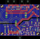
Here's a link to a high-res photo of the area of the board under question (note taken prior to realising my error re C6 and replacement of R6.
R15 is not populated in this board - it is a placeholder for a zero Ohm jumper on the 5V/3V3 boards to bring 12V to their op amp and Vref. (I needed a way to open circuit this part of the 12V board else Z1 and V+ would be connected. R16 is a zero ohm jumper for the 5/3V3 boards for when the level shifter components Z3 and C9 are not populated.)
Re R10, there's much greater noise upstream of R10.
Re Z2 (LM329) I can't reach the cathode but I suspect the answer to the previous question makes this less relevant.
Touching the top of C8 does nothing.
I have had to leave it there for the moment to let the load resistor cool. Nonetheless, it would seem things are narrowing down a little. (Can noise be dumped into the Q1-Q3 cluster from the output of the op amp? I don't believe so but if I am wrong then things could be somewhat circular...) I'm wondering whether to simply start replacing Q1-Q3 (BC807-40) and J1 as I presume the noise will come from such active parts rather than passive resistors. I've poured over the board and can't see any obvious damage or bad solder joints.
(I used an inductor-driven hot plate to do all the SMD soldering, first laying down solder paste with a stencil and placing parts, and then heating until I saw all the paste molten. Not sure if this is relevant.)
Here's a link to a high-res photo of the area of the board under question (note taken prior to realising my error re C6 and replacement of R6.
Last edited:
It sounds like the 10V zener diode Z1 may be the culprit. Perhaps it is being operated at a wildly incorrect current. You could measure the DC voltage across R8 to infer the bias current in the zener. Double check the resistance of R7, R8, and R9 with the ohmmeter -- maybe wrong parts got soldered in those locations. Also doublecheck the pinouts of the PNP transistors, perhaps they are connected incorrectly on the board.
You'll want to replace Z1 with one of your spares, just in case you've got a bad diode or a bad solder joint. While doing so it may be worthwhile to first solder a high value (100nF??) SMD capacitor to those pads, and then solder Z1 onto the capacitor, taking advantage of the wraparound terminals on the cap.
By the way, I am extremely pleased with (this eBay purchase). I bought (8.0 ohms, 1000 watts) and also (4.0 ohms, 1000 watts). I lay the resistor atop a plain red brick on my lab bench and never worry about dangerous overheating. The brick keeps the warm resistor away from the tabletop and scattered papers. Shipping to the US was fast and the transaction was very smooth. I hope it's equally good for UK buyers.
Thanks for the continued help. FWIW I went over every solder joint by hand (reheating some more than once). They appear to be good and it didn't alleviate the problem.
R7, R8 and R9 are all correct (unless mislabelled at the factory).
I will take a look at the SOT-23 Z1. C10 is an AVX MLCC SMD 0.1uF capacitor in 1206/3216M package. Maybe that will work. Thanks.
I bought the 200W version of those resistors (in 8, 6, 4, 2 and 1R) after you pointed them out to me at Parts Connexion (I purchased them on eBay from China).
Last edited:
Now is not the time to trust printed resistor values. Disconnecta de power, discharga de caps, and ohmmeter de resistors. If the universe / Satan can give you a bad zener diode, they can give you bad resistors too. Double check the polarities of C7 and C8. Find a theory to explain why there is an AC waveform across C8.
Understood. Resistors are within tolerance of my cheap multimeter: 35.5R versus 34.8 spec. C7 and C8 polarities are good. After my schoolboy error with C6 I went over everything again and more than once. PNP transistors are good.
Re C8, note I was measuring/examining the waveform on the right side of R11 (the connection from Z2). In any event, I replaced the cap. It is one of the more difficult soldering jobs as I did not enlarge the pads and so perhaps it was a bad joint. I have tested continuity to ground etc and it seems ok.
I have replaced Z1 and added the 0.1uF cap. That wasn't an easy soldering job either.
Unfortunately I need to wait until tomorrow to see if these changes have fixed things.
Thanks again.
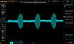
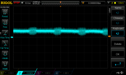
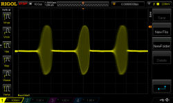
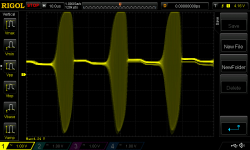
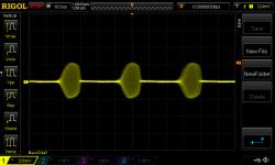
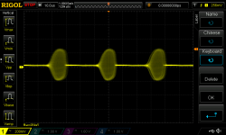
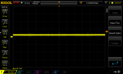
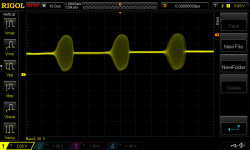
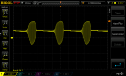
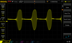
So I did the work above and the issue was still present. I decided to swap out the op amp (I will likely need the soldering practice anyway). No change. I'm wondering if the issue is much further up the chain or some sort of ground loop issue (although I'm clearly way out of my depth trying to figure this out). Here's a few pics:
1. -In of the op amp (or right side of Rx)
2. +In of the op amp
3. GND pin of the op amp
4. Top side of R9 or drain of the pass MOSFET transistor
5. The GND pin hole in the middle of the lower right quadrant of the board
All taken with the scope probe crocodile clip attached to the GND pin at the output caps.
Attachments
Last edited:
I just realised that when I switched scope probes I had the probe at 1x and not 10x when doing the prior tests.
I also tried to do a quick 'heat map' using the scope to take quick max voltage (AC coupled) readings at various points in the circuit. Of course, there was a lot of variance at various circuit points and points of time. So "500" (mV) was anything between, say, 430 and 540. These were quick measurements with the probes alligator clip at the output GND test pin. I'm not sure if these are helpful but it would seem Vref and Vs to the op amp are functioning ok and the PNP transistors don't seem to be the source of the problem.
What's the correct way to probe the rectifier diodes?
Attachments
- Status
- This old topic is closed. If you want to reopen this topic, contact a moderator using the "Report Post" button.
- Home
- Amplifiers
- Power Supplies
- Adventures with 5A regulated voltage circuits