I might be narrowing in the problem - or perhaps it's just obscured the old one (the periodic oscillation) temporarily. I replaced the op amp (and reconfigured the circuit from Zobel to gatestopper, adjusting the compensation resistor Ry to match my modelling). But I had 20V out as it was in last night. Perhaps I did't fry the op amp after all.
It seems the LM329 may have been the problem. See attached for measured voltages at various points in the circuit. With the LM329 in trouble, I don't see the oscillation previously witnessed on the output. Maybe the LM329 is the cause?
Before I replace the LM329 I want to double-check the pin configuration and its resistor value. R10 is 499 Ohms and my LTspice model suggests that this will mean 6.5mA through the LM329 which seems to be straight down the middle of its operating current. When looking at the board, I have the middle pin connecting R10 and R11 and the top pin going to ground.
Yes I agree that the circuit needs debugging before swapping opamps. Even when oscillating, that still should not cause the funny voltages you see. For instance, the pencilled-in voltages at the opamp inputs suggest that the opamp output should be slammed to the pos rail. Is it? Why not? If you open the opamp output, does it slam to the rail? So what is drawing it down?
The LM329 circuit also looks fishy. If you isolate the right side stuff from the 329, does it correctly go to around 6.9V? So what draws it down?
Divide/isolate and concur. Swapping opamps will get you knowhere at this stage.
Is the board really conforming to the schematic?
Edit: what is the value of Rx??
Jan
Last edited:
Hi Jan. Thanks for taking an interest in my travails. Thanks for the tips.
As you will see from post #420 I've identified one problem with the board itself. A sloppy error. And sloppy that I didn't pick it up earlier. A couple of days ago I went through pin configurations on everything except this part. Perhaps I was interrupted, but I missed Z3. I need to think through the ramifications of the current configuration - if Z3 simply sat there (badly configured) is it not the case that there's no DC path from op amp output to gate?
Currently the voltage at the op amp side of R10 is reading 6.95V so I think the replaced LM329 is working fine. The upstream side of the Z1 BZX84-B10 is, however, not reading 10V but rather closer to 9V. Plus I'm expecting to see roughly 0.5V drop across resistors R7-9. (Previously I had too much drop and now it seems not enough.)
Could the reason the op amp isn't slammed to its positive rail be that Q3 is failing, the gate is getting c23V and, as Mark noted earlier, the protection diodes are kicking in?
I need to sleep on it all and pick it up in the morning.
Rx is 732 Ohms.
Last edited:
Yeah I may have been looking at the wrong schematic, the last one I see is in post #601. There the inv input is highest so expect the opamp output to go towards ground. The protection diodes prevent the delta between inv input and non-inv input to get even higher so they work as they should. Or at least one of them does. And that current through the prot diode also goes from pin 3 through that R to the top of the 329 so that is the reason why the ref pin 3 is higher that 6.9V. And with Rx what it is, and Vout what it is, around 10V at the opamp input is perfectly correct as well.
Yet if I see correctly the opamp output is at 10.4V. That's a giveaway - why can't the opamp output go to zero? If it would, it would drawn down the gate and pull it back into regulation.
So I would look at the issue first: why can't the output go all the way down? What's wrong in the output circuit? Is there something connecting it to the pos rail that is too low impedance for the opamp max current it can sink? If you isolate the opamp output, does it dutyfully go towards ground? I bet it does.
Just a question: was the PCB layed-out manually or was there a DRC-link to the schematic?
Jan
Last edited:
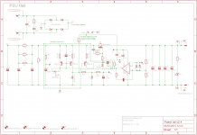
Hi. The full schematic is in #389 and also the relevant parts in #413. It hasn't changed but quick readings of voltages have as I've been working through issues. (I've attached the full circuit again for ease of reference.)
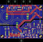
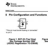
Re your last question, the PCB was laid out in Cadsoft Eagle and passed DRC for the board provider's design rules. Of course DRC doesn't help when one screws up a part's pin configuration. (LM4040 pin configuration attached.) I have attached an image export of the board from Eagle. The Z3 LM4040 problem now seems to blink at me in neon.
I need to think through your other points. I think the issue is that the gate can't be pulled lower because Q3 is failing and holding it at c23V. But why then, as you say, doesn't the op amp output go to zero. Given I have a few spare LM4040 I may just as well correct that issue and see if it narrows things down at least.
EDIT: I guess I could power it up without Z3 in place and check the op amp output?
Attachments
Last edited:
Hi. The full schematic is in #389 and also the relevant parts in #413. It hasn't changed but quick readings of voltages have as I've been working through issues. (I've attached the full circuit again for ease of reference.)
Re your last question, the PCB was laid out in Cadsoft Eagle and passed DRC for the board provider's design rules. Of course DRC doesn't help when one screws up a part's pin configuration. (LM4040 pin configuration attached.) I have attached an image export of the board from Eagle. The Z3 LM4040 problem now seems to blink at me in neon.
I need to think through your other points. I think the issue is that the gate can't be pulled lower because Q3 is failing and holding it at c23V. But why then, as you say, doesn't the op amp output go to zero. Given I have a few spare LM4040 I may just as well correct that issue and see if it narrows things down at least.
EDIT: I guess I could power it up without Z3 in place and check the op amp output?
You could do that.
Or, you could measure across Q3's Re. If it is wide open that is then the cause the opamp can't regulate. That would be a step forward. I guess the purpose of Q3 would be a current source to bias the pass device with the opamp syphoning off the excess bias.
To check, isolate Q3 (lift its Re) and put say 1k from Vin to the gate and let the opamp work. And take out that short across the LM4040.
Jan
Last edited:
Q3 biases Z3 to act as a level shifter in the 12V scenario. (The pass device is a MOSFET. With the 5V and 3V3 versions, yet to be compiled, power to the op amp and Vref circuits is provided by the 12V rail and there's no need for the level shift and a zero Ohm resistor is placed on R16 to close the short when Z3 and C9 are omitted.)
No.Q3 biases Z3 to act as a level shifter in the 12V scenario. (The pass device is a MOSFET. With the 5V and 3V3 versions, yet to be compiled, power to the op amp and Vref circuits is provided by the 12V rail and there's no need for the level shift and a zero Ohm resistor is placed on R16 to close the short when Z3 and C9 are omitted.)
Q3 sends a control voltage to the pass device gate.
The control voltage is modulated by the opamp output. The opamp sinks excess current passed by Q3 to limit the "turn on" of the pass device.
Difference of perspective. In the version where the opamp cannot drive the gate for lack of output headroom, you need something else to bias the gate. Basically that's what Q3 does. The opamp than regulates the exact bias setting at the gate, and you need the level shift to get into the opamp output range.
When the opamp output has enough headroom, it can do the bias itself and you don't need Q3.
So, what's Q3's emitter current?
Jan
When the opamp output has enough headroom, it can do the bias itself and you don't need Q3.
So, what's Q3's emitter current?
Jan
Last edited:
So, what's Q3's emitter current?
Jan
I have replaced (and correctly positioned) Z3. Before I power it up once more and try to answer your question (the last time I checked I was getting an immaterial voltage drop across resistors R7-9 by which I mean if there was any at all it was within the variability of my realtime RMS measurement with my scope) is there anything that can be gleaned from simple resistance measurement of each of Q1-3?
(I have just one NXP BC807-40 left. I will have to order some more and unfortunately off eBay given the small item...)
Jan is asking you this question because your data in post #413 indicates the current might be as high as (22.7 - 21.7)/34.8 = 29 milliamps. This is a lot of current to ask the opamp to sink! Although the AD817 datasheet claims Iout=50mA, other opamps aren't so bodacious. If you were to stick in a NE5534A or a TL071, you'd be screwed. It's also a crazy number because it's the output of a 1-to-1-to-1 current mirror whose input is the Idss of a MMBF5460. Whose datasheet says 1mA < Idss < 5mA. Your measurement data suggesting 29mA, is therefore a red flag.
edit- if you can find a load resistance setting at which there are no oscillations, then you can use a simple DMM to measure the voltage drop ACROSS the PNP emitter resistors. It's pure DC and a DC instrument will give the right answer. Then Ohms Law tells you I = V/R.
edit- if you can find a load resistance setting at which there are no oscillations, then you can use a simple DMM to measure the voltage drop ACROSS the PNP emitter resistors. It's pure DC and a DC instrument will give the right answer. Then Ohms Law tells you I = V/R.
Last edited:
Yes I understand. At that time the voltage drop was excessive. But lmy last tests after various component changes showed this to no longer be the case (albeit my measurements were all taken versus GND and not a direct measurement across the resistor). I am going to check all the solder joints for Q1-3 and J1 again and then I will power it up once more and report back.
Stop reading my mind Mark ")
The other thing that that will most probably materialize is that Q3's base voltage is too low. But let's first clear that huge current we're trying to push down that opamps' throat.
SGK: The best way to trouble shoot is to consistently and logically follow a path from problem to solution. Jumping all over the place rarely gets you to a happy end ;-)
Also understand that homing in on an issue is all about making ONE change at a time, not more, and then see what has changed.
Jan
Last edited:
You know, I just realized that your MOSFET pass transistor does NOT contain any internal zener diodes to prevent VGS from exceeding the ±20 volt datasheet max. Nor does your board design.
So there's a teeny possibility that you may get +22V on the gate while there's +0V on the source, and Poof! goes the gate oxide. This may happen at start-up, and/or it may happen during wild oscillations. Or it may never happen at all, I don't know.
But if crazy, inexplicable behaviors are observed around the MOSFET gate node during initial checkout, debug, and bring-up .... don't forget to suspect that the MOSFET pass transistor may have failed. It could happen.
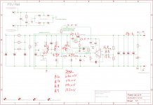
Ok. I powered it up and here's what I get. First I took a quick tour of the board using the alligator clip on my probe attached to the GND pin at the output. (So rough voltages, which of course likely moved a little during the time it took to move around the board.) I have marked them on the circuit.
Secondly, I removed the alligator clip, attached the GND spring and dialled up the resolution on the scope in order to take more accurate measurements of the voltage drops across resistors R6-9. I have listed these below the circuit.
Vin = Vout => the MOSFET is blown? Seems likely to me...
So where to start? Replacing the MOSFET seems sensible but if Q3 again delivers 24V to the gate immediately then it will blow again on startup. Hence my concern regarding incremental changes... Or is most likely that the only reason the voltage is so high there is because of the blown FET?
Attachments
The easiest way to guarantee you won't blow up an NMOSFET pass transistor during debug, is to plug the primary side of your transformer into a Variac and use the Variac to sloooooowly dial up the primary voltage. When the post-rectifier raw DC voltage (across C5) equals 19 volts, stop. Voila, it's impossible to put 20V across your MOSFET when there's only 19 volts to work with.
It does seem that perhaps your opamp isn't doing its job. When VIN- exceeds VIN+ the opamp is supposed to slam its output pin down as low as possible. On the other hand if the Nchannel MOSFET is a big solid short from drain to gate and gate to source, then the 50mA opamp is fighting against the 100A MOSFET and I know who I'm betting on.
One way to proceed is to simply install a new MOSFET and hope for the best.
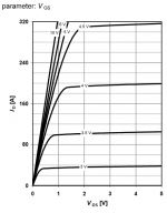
Another way to go is to solder a pair of thru hole zener diodes in series (anode to anode) and tack solder this gizmo across the gate and source of a new MOSFET. Looking at the datasheet figure copied below, it seems you will get all the current you want (5A) with VGS < 5V so you could buy 4.7V zener diodes. Even if they have to drink the entire 50mA output current of the AD817 opamp that's less than half a watt.
Yet another way to go is to notice that the pins of the MOSFET are ordered G, D, S. Hmmm, the pins of a power NPN bipolar are B, C, E. Hmmm. So if you ran the damn thing with an easy load and a low output current, for debug purposes, you could use a TO220 power NPN instead of the TO220 MOSFET. Maybe a power NPN will not explode itself. Maybe a power NPN will let you debug your VREF network and your opamp feedback network. Then once you've got all that figured out and Known To Be Good, you can yank out the NPN and put back your MOSFET. Then see if it continues to work with the MOSFET like it worked with the NPN. I assume you have some D44H11 power NPNs from the Jung/Didden Super Regulator, lying around.
Which of these do I favor? Variac + brand new MOSFET. But then I already own a Variac.
It does seem that perhaps your opamp isn't doing its job. When VIN- exceeds VIN+ the opamp is supposed to slam its output pin down as low as possible. On the other hand if the Nchannel MOSFET is a big solid short from drain to gate and gate to source, then the 50mA opamp is fighting against the 100A MOSFET and I know who I'm betting on.
One way to proceed is to simply install a new MOSFET and hope for the best.
Another way to go is to solder a pair of thru hole zener diodes in series (anode to anode) and tack solder this gizmo across the gate and source of a new MOSFET. Looking at the datasheet figure copied below, it seems you will get all the current you want (5A) with VGS < 5V so you could buy 4.7V zener diodes. Even if they have to drink the entire 50mA output current of the AD817 opamp that's less than half a watt.
Yet another way to go is to notice that the pins of the MOSFET are ordered G, D, S. Hmmm, the pins of a power NPN bipolar are B, C, E. Hmmm. So if you ran the damn thing with an easy load and a low output current, for debug purposes, you could use a TO220 power NPN instead of the TO220 MOSFET. Maybe a power NPN will not explode itself. Maybe a power NPN will let you debug your VREF network and your opamp feedback network. Then once you've got all that figured out and Known To Be Good, you can yank out the NPN and put back your MOSFET. Then see if it continues to work with the MOSFET like it worked with the NPN. I assume you have some D44H11 power NPNs from the Jung/Didden Super Regulator, lying around.
Which of these do I favor? Variac + brand new MOSFET. But then I already own a Variac.
Attachments
I don't own a variac but I also don't mind sacrificing a power MOSFET in an attempt to make some progress here.
Anode to anode? Don't I need cathode at the gate and anode at the source, two in series, anode to cathode, for c10V (or simply a single 10V zener given if I solder at the MOSFET then the span is narrow)?
What do people think about the current source operation? I was expecting a tighter range of voltage drops across R7-9. Obviously there may be measurement variance and resistance variance (while spec'd at 34.8R my cheap multimeter measures 35.2R but the same for each). The fact that Z1 is sitting at 9V and not something closer to 10V is bugging me.
(I'm also very puzzled as to how I got 12V output prior to disintegrating my chop chop box when I had a short at Z3. But I can leave that for another day if need be.)
Another way to go is to solder a pair of thru hole zener diodes in series (anode to anode) and tack solder this gizmo across the gate and source of a new MOSFET. Looking at the datasheet figure copied below, it seems you will get all the current you want (5A) with VGS < 5V so you could buy 4.7V zener diodes.
Anode to anode? Don't I need cathode at the gate and anode at the source, two in series, anode to cathode, for c10V (or simply a single 10V zener given if I solder at the MOSFET then the span is narrow)?
What do people think about the current source operation? I was expecting a tighter range of voltage drops across R7-9. Obviously there may be measurement variance and resistance variance (while spec'd at 34.8R my cheap multimeter measures 35.2R but the same for each). The fact that Z1 is sitting at 9V and not something closer to 10V is bugging me.
(I'm also very puzzled as to how I got 12V output prior to disintegrating my chop chop box when I had a short at Z3. But I can leave that for another day if need be.)
My advice: remove Q3 - its biasing stuff at the left looks pretty dodgy. Mark also has made some pertinent comments there.
Connect 1k between Vin and gate and that should get the regulator working.
THEN start with a fresh look at the bias stuff knowing that the reg is fine.
Can you also do the DC measurements with a multi meter instead of with a scope? It's confusing to see the values change with every time you do the measurements.
Jan
- Status
- This old topic is closed. If you want to reopen this topic, contact a moderator using the "Report Post" button.
- Home
- Amplifiers
- Power Supplies
- Adventures with 5A regulated voltage circuits