About OPA1656 DC output offset: depending on gain, a low level circuit with the OPA1656 can show a few mV as output offset.
I have a circuit with two OPA1656's and it so happens that one offset is subtracted from another and almost cancels - in LTspice. Of course that is because in LTspice all instances of the device are identical.
How would that be in the real world? If I use two OPA1656's in a common package (it's a dual, after all), can I expect the offset voltages of the two opamps in the same package to track somewhat, fairly well, or not at all?
Jan
From the offset spec's:
OPA1656 : ±500V
OPA827 : ±75uV
other OPAMP's : to come...
Also keep in mind, the cross talk from the OPA656 CANNOT be simulated within LTSPICE (may as other spice SW)...
Also using LTSPICE, the noise analysis shows a far more rising noise (on an active Notch circuit) than using the OPA827. May it is the model dependent...
Also, for a measurement gear, I would not use unknown chip cross talks
Hp
Hans-Peter, this is not about the autoranger. ;-)
In LTspice, the OPA1656 model appears to have a fixed input offset of 0.5mV. So in a circuit that subtracts two stages, you get almost perfect 0V offset, but in reality two opamps will not have exactly the same offset. Hence my question. Maybe Johnc124 can chime in.
BTW is there a dual of the OPA827? ;-)
Jan
Last edited:
Marcel, that is interesting. I am no expert in IC layout (you are). My guess was that offset is a result of a process variable, which might be the same on the other opamp on the same die.
So, I can't gain anything in this context by using a dual rather than 2 separate opamps?
BTW The OPA828 seems a worthwhile upgrade to the '827.
Jan
So, I can't gain anything in this context by using a dual rather than 2 separate opamps?
BTW The OPA828 seems a worthwhile upgrade to the '827.
Jan
Last edited:
One would normally try to design an op-amp such that the offset is dominated entirely by random local variations between supposedly equal devices, mainly random local variations between the two input transistors. As the variations are random and very local, an op-amp at the other side of the same chip will have its own offset.
It's a different matter when you look at the input bias current of a bipolar op-amp without base current compensation, for example. That's simply half the tail current of the input pair divided by hFE + 1, and as transistors on the same chip have very similar hFE values, the bias currents of two op-amps on the same chip will match reasonably well.
On a bipolar op-amp with base current compensation, you try to get rid of the base current by making a circuit that injects an equal but opposite current. Mismatch due to random local variations between the input transistors and those in the base current compensation circuit will result in a small remaining bias current. As that remaining bias current comes from random local variations, it won't match with an op-amp on the other side of the chip.
If a circuit designer or a layouter has done something stupid that results in a large systematic offset, on top of the inevitable offset due to random local variations, then you get a strong correlation between the offsets of two op-amps on the same chip. For a CMOS op-amp, an example would be to place one input transistor right next to the edge of an N-well and the other input transistor not: the different surroundings will result in slightly different transistor behaviour, so the VGS of one transistor doesn't properly cancel the VGS of the other transistor anymore.
Last edited:
Jan, in post #31 of this thread, JohnC says the OPA1656 is NOT trimmed for input offset voltage. So you can remove "systematic errors in trimming procedure" from the list of possible explanations how two opamps on the same die MIGHT have input offset voltages which are correlated.
The circuit design and layout are carefully executed to remove ALL systematic sources of offset voltage. If they are successful, then the only remaining sources are non-systematic, i.e., random. As Marcel has told you.
Post #31 tells you of a similar opamp which IS trimmed. That one will have far lower input offset voltage -- perhaps not zero but far lower -- and its manufacturing tests will be more expensive. This additional cost will be included in the price.
Yes, apparently has to do with the P-input pair is active together with the N-pair in that region.
https://e2e.ti.com/support/amplifiers/f/14/t/818590
https://e2e.ti.com/blogs_/archives/...4/16/rail-to-rail-inputs-what-you-should-know
Jan
https://e2e.ti.com/support/amplifiers/f/14/t/818590
https://e2e.ti.com/blogs_/archives/...4/16/rail-to-rail-inputs-what-you-should-know
Jan
Last edited:
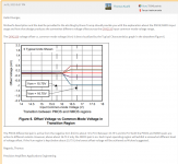
Yes, we call that behavior on the OPA2156 input crossover distortion and it is present on all op amps which use a dual input stage to achieve rail-to-rail input voltage range. A non-rail to rail input opamp (like OPA1656) would just clip at that voltage, so pick your poison. We do have some 5V op amps with "zero crossover distortion" input stages, which is just a single input pair with a charge pump to achieve rail-to-rail input specs, but we haven't done that in a HV op amp yet, and as the tail current increases to achieve lower voltage noise, the penalty of the charge pump's efficiency is more and more painful...Certain HV op amps have both input stages trimmed, which reduces the step, but there is still a discontinuity (OPA192 is an example of this).
Others have commented correctly on the matching of offset voltages in a dual channel op amp. I even put a histogram of this in the OPA1692 datasheet (Figure 2, input offset delta) and you can see that the standard deviation is sqrt(2) times the measurement of a single device. Theoretically you could improve this by doing the layout of the die so that the input stages were both in a common-centroid (essentially inside of each other), but you'd probably pay a lot of other penalties for doing this like degraded crosstalk, and it would probably be more difficult to do a proper thermal layout of both channels.
Others have commented correctly on the matching of offset voltages in a dual channel op amp. I even put a histogram of this in the OPA1692 datasheet (Figure 2, input offset delta) and you can see that the standard deviation is sqrt(2) times the measurement of a single device. Theoretically you could improve this by doing the layout of the die so that the input stages were both in a common-centroid (essentially inside of each other), but you'd probably pay a lot of other penalties for doing this like degraded crosstalk, and it would probably be more difficult to do a proper thermal layout of both channels.
Others have commented correctly on the matching of offset voltages in a dual channel op amp. I even put a histogram of this in the OPA1692 datasheet (Figure 2, input offset delta) and you can see that the standard deviation is sqrt(2) times the measurement of a single device. Theoretically you could improve this by doing the layout of the die so that the input stages were both in a common-centroid (essentially inside of each other)
Why would using a single common centroid layout for the input transistors of both op-amps result in a better matching of offset voltages than using separate common centroid layouts for each op-amp input stage?
The mismatch between the offset voltages is something like VGS1a - VGS1b - (VGS2a - VGS2b), where I've called the input transistors of the first op-amp 1a and 1b and those of the second op-amp 2a and 2b and neglected any source of offset other than input transistor mismatch. As long as VGS1a and VGS1b match well and VGS2a and VGS2b match well, I don't see why it would help to also layout for optimal matching between VGS1a,b and VGS2a,b.
Thanks John, that 1692 looks good as well. Time to study and sim!
What intrigues me is the increase in open loop output impedance for lower frequencies. What is the mechanism behind that?
Jan
Output impedance at low frequencies tends to decrease as frequency increases because the compensation capacitor creates a local loop around the output stage, reducing its output impedance. The magnitude of this effect really depends on the internal compensation scheme.
OPA1692 was designed for low power applications (battery powered mics for example) so you have to view its performance in the context of its power supply current (like all op amps). That being said, the low power requirement forced us to get innovative and find some really cool ways to reduce distortion without wasting power.
On my common centroid comment, I admit it's more my gut instinct that if you put the two input stages together in a higher-ordered common centroid layout you could get better matching. One mechanism is indeed that you could better guarantee that all transistors are at the exact same temperature. But also it would give better matching in spite of local gradients in the various processesing steps. But again, I'm just guessing here, if one of you guys could pony up and buy a million of them, I could have one of my teams try it out!
Why would using a single common centroid layout for the input transistors of both op-amps result in a better matching of offset voltages than using separate common centroid layouts for each op-amp input stage?
Because the channel carriers mobility depends strongly on the temperature, and the offset goes as 1/mobility. Different temperatures for the inputs, different offset voltages.
Sorry, can't type equations here, but start from the fundamental Vgs=f(Idrain), calculate delta Vgs, you'll see that the offset (DVgs)^2~1/mobility.
The situation is worse for MOSFETs compared to bipolars, since the electron mobility in MOSFETs varies as T^(-2.4) due to multiple scattering effects, while the bipolar saturation current varies only as approx T^(-1.5), plus the sqrt vs. logarithmic dependency of V=f(I).
Last edited:
- Home
- Vendor's Bazaar
- OPA1656: High-Performance CMOS Audio Op Amp