I got interested reading through this last night and wondered how you got on...
This is my thinking...
Have you checked the cathode resistor of V6 and other associated parts and connectivity of those parts. Wouldn't a an open circuit R83 or open or high resistance path here cause the cathode to assume a high voltage and hence transfer that via the FET to the anode of V5?
Given that V4 anode volts is correct I'm assuming the cathode voltage is also correct which is shown as around 12 volts on the diagram.
The 1k grid resistors see no voltage across them and are far to low in value to have any concerns over noise contribution or other qualities. Any 1k of similar physical size. Manual says 0.6w which is a standard small rating. 0.25w would be fine as well as no power is dissipated here.
Attachments
Hey - thanks for helping out with some more brain power.
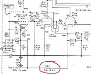
I have measured R83 in circuit and it's 32.5K on the RHS and 30.5 on the LHS.
I am only using logic and measurements in situ before unsoldering everything, but the R27 2.7K is 1.95k on both sides and for the life of me I can't find R28...but it's all a bit of a mystery to me!!
These were the voltages on this resistor, can't recall which side I tested
33k 12v RH
33k 21v LH
Thanks!
Measuring parts in circuit can be fraught with difficulties due to interactions with other circuitry.
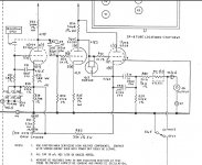
I would measure the voltage from ground to each end of R83. On the faulty channel you mentioned having 350v on the 'single leg of the FET' which is the gate and which goes to the cathode of V6.
So the 350 volts you measured should be present on one end of R83.
You must check the voltage on the other end of R83. What is it? It should be around 12 volts.
You have to check resistors out of circuit but you only need lift one end to do this, no need to totally remove.
Also...
The stage around V5 is self contained and self biased.
If you remove the FET and remove V6 (diagram shows V6 heaters are not in a chain so no problem doing this) then the anode of V5 should bias up to the correct voltage.
If it doesn't and it is still high then you next remove the 1k grid resistor in case the valve socket of V6 is electrically leaky/carbonised and there is a conduction path there.
If the voltage on V5 anode is then normal after lifting the 1k then you are looking at leakage around the socket of V6 and/or the board/wiring itself.
Interesting fault, I'll look in later")
(I also note the coupling cap C10 is shown as 250 volt and you have more than that present with this fault... as long as you have nothing connected to the output then with just a 475k to ground it will probably be OK)
The stage around V5 is self contained and self biased.
If you remove the FET and remove V6 (diagram shows V6 heaters are not in a chain so no problem doing this) then the anode of V5 should bias up to the correct voltage.
If it doesn't and it is still high then you next remove the 1k grid resistor in case the valve socket of V6 is electrically leaky/carbonised and there is a conduction path there.
If the voltage on V5 anode is then normal after lifting the 1k then you are looking at leakage around the socket of V6 and/or the board/wiring itself.
Interesting fault, I'll look in later
(I also note the coupling cap C10 is shown as 250 volt and you have more than that present with this fault... as long as you have nothing connected to the output then with just a 475k to ground it will probably be OK)
should say 30.5K on LHS oops
If in doubt then lift one end and measure.
Quick and dirty checks (beware shock hazard) are to see if a resistor with lots of voltage across it is getting hot. If you have 300 volts across a 33k its going to be hot. So if it is much hotter than the one with only 150 volts or so across it then chances are it is OK.
Measurement is best though.
I am almost certain to spoil the 1k grid resistor on removal, any suggestions of good quality replacements?
Just leave the grid resistor in place. The other notes will still apply.
The 33k resistor on LH does get hot.
Pin3 V4 LH 11-14v and then stablising at 13.25v or so, pin 8 V4 (RH) 19.7v but can vary quite a bit oscillating around.
I will follow the test advice later, and take the FET out of circuit.
That does seem the next logical step (and remove V6 as well). Then see what V5 biases up to on the anode.
The below test done with V6 not plugged in
B+1 pretty much still on spec at 401v
180v V4 RH 300K across anode resistor (socket 1)
40v V5 RH 300K across anode resistor (socket 6)
180v V4 LH 301K across anode resistor (socket 6)
175v V5 LH 300k across anode resistor (socket 1)
so now the FET is OOC on LH channel, which has put the measured resistance back to 300k, and the correct voltage, BUT the RH channel is now down on one of the anodes.....any ideas.
I could take this side FET out now, and make the assumption that the FETs are not able to pass sufficient current as they are considerably lower spec as the are not AN4562, but actually now replaced as AN4650 on all 4 including this RH channel still in circuit?
am I going mad?
What do you think?
The right channel was always OK I think... so I wouldn't worry at this stage on that... although I have no immediate explanation for what you are seeing there. The stage around V5 is self contained.
All I could suggest initially is to put that section back as it was and confirm it is back to normal voltages on what was the good channel. Make sure you haven't blobbed any solder between the gate and the other pins.
So your left channel is now correct with the FET and V6 removed. You should also be seeing around 12 volts on the empty pin of the socket that the cathode of V6 connects to in this condition.
There should also be zero (0.00) volts across the 33k with V6 and the FET removed.
As to the FET's... I'm not sure what these do. The other versions have diodes here and in normal operation they are reverse biased and do nothing. The FET is actually wired to act like a low leakage diode.
If there is doubt on these FET's then why not swap them out for diodes, at least as a test.
All I can think they do is to clamp the G-K voltage at start up (or power off) and so prevent V6 from conducting to heavily and putting to high a voltage on the cathode (and the 250v rated coupling caps).
I can't see they do anything else.
ok - some more measurements,
still looking weird...
27 v across RH 33k
0v on LH 33k
40V on pin 8 valve 6 cathode RH (to earth)
1.4v on pin 3 valve 6 cathode LH (to earth)
RH 33k 3.6V to earth and 40V to earth (valve side) LH 33k 1.4V, 1.4V
2 pins to the single pin unconnected FET measures 250 ohms (resitance across the FET as diode)
Firstly FET's are difficult to measure unless you understand how they work. The gate impedance is so high that measuring across the device from drain to source can give wildly varying readings as the gate picks up stray charge. Just touching the gate with a finger can 'pinch off' the FET and it then appears as an open circuit. Touch it again and you might turn the device on and now the drain to source channel reads quite low, perhaps as low as a few tens of ohms.
Lets just recap on what should happen. Concentrate on one channel at a time otherwise it gets really confusing. Lets build it up in stages.
V5 is self contained and self biased. If you remove the FET and remove V6 then the stage should bias up to the voltages shown give or take. So that is the starting point. You need to see around 150 volts on the anode of V5 in this initial state.
Lets try and cover all bases here. Is it possible there is a problem with the (to me) under rated coupling cap C10 (and lets not discount the parallel C43)?
Lets isolate these two caps and leave them isolated until the thing is fixed
The reasoning for that is that if the switch SW5 is in 'mute' and if there is leakage in one of those caps then that would tend to pull the cathode volts down and upset the whole chain.
So lets take them out of the equation and isolate them.
V6 is just a buffer stage. Having got the correct voltage on V5 anode (150v or so) then V6 when placed back in circuit should bias up to the voltage shown. The anode volts of V5 should appear on the grid of V6. I would suggest leaving the FET out of circuit while doing this.
The cathode of V6 should be as shown at around 160v.
Try following that and that and see where we get to.
Lets just recap on what should happen. Concentrate on one channel at a time otherwise it gets really confusing. Lets build it up in stages.
V5 is self contained and self biased. If you remove the FET and remove V6 then the stage should bias up to the voltages shown give or take. So that is the starting point. You need to see around 150 volts on the anode of V5 in this initial state.
Lets try and cover all bases here. Is it possible there is a problem with the (to me) under rated coupling cap C10 (and lets not discount the parallel C43)?
Lets isolate these two caps and leave them isolated until the thing is fixed
The reasoning for that is that if the switch SW5 is in 'mute' and if there is leakage in one of those caps then that would tend to pull the cathode volts down and upset the whole chain.
So lets take them out of the equation and isolate them.
V6 is just a buffer stage. Having got the correct voltage on V5 anode (150v or so) then V6 when placed back in circuit should bias up to the voltage shown. The anode volts of V5 should appear on the grid of V6. I would suggest leaving the FET out of circuit while doing this.
The cathode of V6 should be as shown at around 160v.
Try following that
and that and see where we get to.Attachments
Did I miss something?
The schematic in Post # 35.
The JFET is drawn as a P-Channel JFET.
An N-Channel JFET, would have to be connected the other way, with the gate to the grid stopper . . .
The only reason for the JFET to be connected from the grid stopper resistor to the cathode is to prevent the grid from going more than about 0.6V positive than the Cathode.
That JFET is nothing more than a Diode when connected that way.
A Common Signal Diode would provide the same protection, but would have Much Less capacitance when at 0V or less (reverse biased).
And, for normal operation, the JFET and signal diode will be working from 0V to reversed bias voltages.
The higher capacitance of the JFET (compared to the signal diode), could cause high frequency roll-off.
Simple . . . signal diodes are less expensive, lower capacitance, and usually higher reverse voltage breakdown than a JFET.
Use the solid state device of your choice, but make the choice when you understand the tradeoffs.
Hint: make sure that both the Drain and the Source are connected together. And the Gate to the other point of the circuit.
Last edited:
Mooly, thanks again I picked up your note after I had already posted my last.
so the plan is I will remove FET on LH channel again, put in V6 and power up and test voltages? The part that confuses is me is what I do with the capacitors C10 and C43 in this trial as I am not sure what isolating these actually means - just disconnect on one end?
If I do this then how do I get output across to R29/
- Status
- This old topic is closed. If you want to reopen this topic, contact a moderator using the "Report Post" button.
- Home
- Amplifiers
- Tubes / Valves
- Hiss on 1 channel ideas