Yep fine - if you have built it make sure you have a few JFET's to hand so you can match. You can tie the gate to 0v and with a suitable source resistor (about the same current as in the CCS/2) get two with the same source voltage. There will be a big spread. That's the trouble with simulation everything is matched and looks good.
Last edited:
GNF to the second jfet will work well - its exactly what I did with the EL184 LTP. You can add a dominant pole by placing a series R+C between the two gates of the jfets. Looks an odd thing to do but gets round losing the drive at HF. Across the plates of the LTP will also work but you may run out of drive.
Last edited:
I've asked to the guy I bought it from, and he told me he bought fifty 2SK170GR and then he matched best ones by transconductance.Yep fine - if you have built it make sure you have a few JFET's to hand so you can match.
Like a Zobel but connecting the input of the stage instead of the output. Thanks!GNF to the second jfet will work well - its exactly what I did with the EL184 LTP. You can add a dominant pole by placing a series R+C between the two gates of the jfets.
Yes, this evening I will post the schematic and the simulation as well.
Tomorrow afternoon I will try some of these mods and report here the results.
The 7 kOhm Raa anche the cathode feedback have been two big improvements on the overall sound.
Tomorrow afternoon I will try some of these mods and report here the results.
The 7 kOhm Raa anche the cathode feedback have been two big improvements on the overall sound.
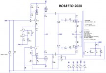
The schematic is attached:
- 12ax7 plate resistor is 120k;
- 12ax7 grid voltage divider is 220k 10k;
- CCS is set at 1.2 mA (600 uA per side);
- jfet are LSK170B;
- driver cathode resistor is 150k;
- RC feedback from driver's cathode to nfb jfet gate is 1u + 270k (gate resistor to ground is 1k);
- EL34s grid leak are 82k;
- EL34s have 40%UL + 0-4 and 4-16 Ohm secondary OPT used as cathode feedback;
- gnfb is 33 kOhm ||47 pF
- EL34 grid stopper is 1 kOhm, screen stopper is 100 Ohm;
This is the harmonic content at 1 Wrms (140 mVrms at input), almost nothing:
This is the harmonic content at 16 Wrms (560 mVrms at input), very low and only 2nd and 3rd:
This is the harmonic content at 33 Wrms (850 mVrms at input), basically 3rd only:
- 12ax7 plate resistor is 120k;
- 12ax7 grid voltage divider is 220k 10k;
- CCS is set at 1.2 mA (600 uA per side);
- jfet are LSK170B;
- driver cathode resistor is 150k;
- RC feedback from driver's cathode to nfb jfet gate is 1u + 270k (gate resistor to ground is 1k);
- EL34s grid leak are 82k;
- EL34s have 40%UL + 0-4 and 4-16 Ohm secondary OPT used as cathode feedback;
- gnfb is 33 kOhm ||47 pF
- EL34 grid stopper is 1 kOhm, screen stopper is 100 Ohm;
This is the harmonic content at 1 Wrms (140 mVrms at input), almost nothing:
Code:
Harmonic	Frequency	 Fourier 	Normalized	 Phase  	Normalized
 Number 	  [Hz]   	Component	 Component	[degree]	Phase [deg]
    1   	1.000e+03	3.966e+00	1.000e+00	   -1.00°	    0.00°
    2   	2.000e+03	2.826e-04	7.125e-05	  129.46°	  130.47°
    3   	3.000e+03	1.624e-04	4.096e-05	  171.85°	  172.85°
    4   	4.000e+03	9.218e-05	2.324e-05	 -173.48°	 -172.48°
    5   	5.000e+03	7.195e-05	1.814e-05	  179.97°	  180.97°
    6   	6.000e+03	6.114e-05	1.542e-05	 -177.77°	 -176.76°
    7   	7.000e+03	5.414e-05	1.365e-05	 -179.90°	 -178.90°
    8   	8.000e+03	4.584e-05	1.156e-05	 -179.72°	 -178.72°
    9   	9.000e+03	4.191e-05	1.057e-05	 -179.88°	 -178.88°
Total Harmonic Distortion: 0.009107%(0.009551%)
This is the harmonic content at 16 Wrms (560 mVrms at input), very low and only 2nd and 3rd:
Code:
Harmonic	Frequency	 Fourier 	Normalized	 Phase  	Normalized
 Number 	  [Hz]   	Component	 Component	[degree]	Phase [deg]
    1   	1.000e+03	1.587e+01	1.000e+00	   -1.01°	    0.00°
    2   	2.000e+03	4.628e-03	2.916e-04	   99.87°	  100.88°
    3   	3.000e+03	3.550e-03	2.237e-04	  157.61°	  158.62°
    4   	4.000e+03	4.107e-04	2.588e-05	 -157.37°	 -156.36°
    5   	5.000e+03	1.015e-03	6.397e-05	  178.61°	  179.62°
    6   	6.000e+03	2.768e-04	1.744e-05	  155.08°	  156.09°
    7   	7.000e+03	9.420e-05	5.935e-06	    5.23°	    6.23°
    8   	8.000e+03	2.356e-04	1.485e-05	 -142.37°	 -141.37°
    9   	9.000e+03	2.868e-04	1.807e-05	 -179.77°	 -178.76°
Total Harmonic Distortion: 0.037509%(0.037689%)
This is the harmonic content at 33 Wrms (850 mVrms at input), basically 3rd only:
Code:
Harmonic	Frequency	 Fourier 	Normalized	 Phase  	Normalized
 Number 	  [Hz]   	Component	 Component	[degree]	Phase [deg]
    1   	1.000e+03	2.298e+01	1.000e+00	   -1.04°	    0.00°
    2   	2.000e+03	4.777e-03	2.079e-04	  115.35°	  116.38°
    3   	3.000e+03	5.535e-01	2.409e-02	    0.38°	    1.42°
    4   	4.000e+03	1.883e-02	8.195e-04	   90.04°	   91.07°
    5   	5.000e+03	1.789e-01	7.786e-03	  179.70°	  180.74°
    6   	6.000e+03	1.252e-02	5.447e-04	  -90.95°	  -89.92°
    7   	7.000e+03	2.088e-02	9.089e-04	 -176.71°	 -175.68°
    8   	8.000e+03	3.935e-03	1.712e-04	  -98.07°	  -97.03°
    9   	9.000e+03	2.828e-02	1.231e-03	    1.60°	    2.63°
Total Harmonic Distortion: 2.538261%(2.539844%)
Attachments
I guess your taking some of the feedback from the driver cathode for stability. If you want the lowest distortion then it should come from the output. What about reducing the 1u with the 270k so that only the HF comes from the driver cathode. Just an idea. However the distortion looks very good on simulation. Are you building it in parallel and testing your ideas there?
Last edited:
I take the signal both from the cathode of the driver and from the output.
The idea is to have short/local feedback paths inside a bigger feeeback path.
What would be the benefit of having feedback on high frequencies only?
The idea is to have short/local feedback paths inside a bigger feeeback path.
What would be the benefit of having feedback on high frequencies only?
Please look at the math:
Suppose I have 2 exactly matched JFETs, 1.000mA each; the total is 2.000mA
Suppose the BJT current source is 2.050mA (2.000ma + 50uA).
Then the BJT voltage will be less than its minimum required burden voltage (saturated).
Suppose I have 2 exactly matched JFETs, 1.000mA each; the total is 2.000mA
Suppose the BJT current source is 1.950mA (2.000ma - 50uA).
Then the BJT voltage drop will be very large.
And the JFETs and 12AX7 cathodes will be current starved.
And now the solution:
Suppose I have 2 exactly matched JFETs, 1.000mA each; the total is 2.000mA
Suppose the BJT current source is eactly 2.000mA.
Everything is wonderful! Good!
Until . . .
The temperature changes by 1 Degree, then the BJT and JFET current sources change at different rates (and in different directions, yes?).
JFET currents go Down with rising temperatures.
BJT currents go Up with rising temperatures.
Does the simulation software account for this?
Did I miss something?
Suppose I have 2 exactly matched JFETs, 1.000mA each; the total is 2.000mA
Suppose the BJT current source is 2.050mA (2.000ma + 50uA).
Then the BJT voltage will be less than its minimum required burden voltage (saturated).
Suppose I have 2 exactly matched JFETs, 1.000mA each; the total is 2.000mA
Suppose the BJT current source is 1.950mA (2.000ma - 50uA).
Then the BJT voltage drop will be very large.
And the JFETs and 12AX7 cathodes will be current starved.
And now the solution:
Suppose I have 2 exactly matched JFETs, 1.000mA each; the total is 2.000mA
Suppose the BJT current source is eactly 2.000mA.
Everything is wonderful! Good!
Until . . .
The temperature changes by 1 Degree, then the BJT and JFET current sources change at different rates (and in different directions, yes?).
JFET currents go Down with rising temperatures.
BJT currents go Up with rising temperatures.
Does the simulation software account for this?
Did I miss something?
Last edited:
OK this is more difficult to explain. Local feedback paths can be used to linearise part of the design without causing instability as the phase lag of the local paths is much smaller. So I think thats what you have done. If you decrease the 1uF to much smaller then you can take more feedback from the speaker at the lower frequency, and then as the phase lag gets large through the transformer (>20KHz) you start to take more signal from a local path helping with stability. Its a common thing to do with op-amps if your driving like an external buffer.
The simulator will account for this but only if you for example change the CCS by 10% and then see what happens. It only tells you what you want to know. I suspect you are correct in that the circuit does have this flaw and the operating point is very sensitive. Your not actually setting the JFET voltage you are telling the JFET to operate at a certain current and letting the source-gate voltage adjust to get to that current. The JFET is not actually a current source here. The two requirement are that the FET's are well matched and CCS does not forward bias the gate-source so you need to look at min ids when vgs = 0v
Last edited:
Thanks 6A3sUMMER, the answer to your question is easy: No, it doesn’t.
I know simulations have tons of limitations.
I also know that the experience of skilled EEs has no price, and this is one of the best places to learn and share ideas.
I know simulations have tons of limitations.
I also know that the experience of skilled EEs has no price, and this is one of the best places to learn and share ideas.
Thanks Baudoin0 for the explanation on nfb at different frequencies, I was not aware of this trick. It will takes me a bit more to test it, but is something more I know. Thanks
How can it be solved?I suspect you are correct in that the circuit does have this flaw and the operating point is very sensitive.
Think its fine. As long as the fets are accuarely matched and the CCS < Ids(min) when Vgs=0V things are OK. Sorry. So for your 2sk170 this is 2.6ma
Last edited:
Your not actually setting the JFET voltage you are telling the JFET to operate at a certain current and letting the source-gate voltage adjust to get to that current. The JFET is not actually a current source here. The two requirement are that the FET's are well matched and CCS does not forward bias the gate-source so you need to look at min ids when vgs = 0v
It seems to me that the total current is fixed, but not the individual current through each jfet. Each jfet has approximately the same drain-source voltage and gate-source voltage (not withstanding the effect of the source resistors), current under those conditions will depend on the particular device. Mismatching will show up as differing current in each leg, which will result in different anode voltages for the 12AX7's.
Can be fixed with a balance pot instead of fixed source resistors.
- Home
- Amplifiers
- Tubes / Valves
- improvements on 12AX7 12AT7 EL34 schematic?