@steveu you should probably know that this topology was used in production amps in the 70s.. so obviously it doesnt work :/
LT1166 for bias control is not that old
")
LV's amp
LV made it work by using a lot of positive feedback, and just a bit more negative feedback. This also floats the inputs so there is no common mode range problem. But the I.H. circuit +in is grounded so if it worked at all, it would clamp at +-4V when the floating rails hit zero VDC. It would probably latch up. The +-inputs must stay within the rail voltages. But some spice models do not model the rails properly, so a simulation gives false results.
Driving the LT1166 outputs may work, but not well, as others have described.
I see, you are talking about post #5 and #6 - Ian H. simulations.
It looks like the op-amp is floating, like Elvee's current dump amp.
I built the 1st current dump amp (the 'active' one), but I couldn't make the 2nd one ('passive' version) stable...
LV made it work by using a lot of positive feedback, and just a bit more negative feedback. This also floats the inputs so there is no common mode range problem. But the I.H. circuit +in is grounded so if it worked at all, it would clamp at +-4V when the floating rails hit zero VDC. It would probably latch up. The +-inputs must stay within the rail voltages. But some spice models do not model the rails properly, so a simulation gives false results.
Driving the LT1166 outputs may work, but not well, as others have described.
Ian circuit
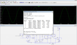
So, it seems Ian's LT1166 model has problems, which I am unlikely to resolve. BUT, LTSpice (now?) comes with a working LT1166 model in "special functions". Using that model, Ian's circuit works quite well. Except, he is mostly driving the LT1166 outputs. Vin is slightly driven out of phase?? With a 2.5V input, I get about 0.002%THD @ 1KHz.
So, it seems Ian's LT1166 model has problems, which I am unlikely to resolve. BUT, LTSpice (now?) comes with a working LT1166 model in "special functions". Using that model, Ian's circuit works quite well. Except, he is mostly driving the LT1166 outputs. Vin is slightly driven out of phase?? With a 2.5V input, I get about 0.002%THD @ 1KHz.
LT1166 for bias control is not that old
Yeah I misread when tired, I thought he was referring to the opamp. The thread is so long i mustve missed where the LT1166 was tried!
So, it seems Ian's LT1166 model has problems, which I am unlikely to resolve. BUT, LTSpice (now?) comes with a working LT1166 model in "special functions". Using that model, Ian's circuit works quite well. Except, he is mostly driving the LT1166 outputs. Vin is slightly driven out of phase?? With a 2.5V input, I get about 0.002%THD @ 1KHz.
Hi steveu,
My Post 37 explains differences in the LTspice models for the LT1166. Use the LTspice XVII library model. But if it fails to start then try my model (that's why I made it slightly different).
Re driving the LT1166 outputs. Post 27 covers this. As far as I can work out there's no problem injecting current into these outputs such as from an opamp or VAS stage. Look at the simplified internal circuit in the datasheet and the input stage drives the autobias circuit with current as well.
But the LT1166 input stage does not cause cross-conduction issues at very high frequencies like an opamp can that drives the top/bottom pins. So if you use an opamp to drive the top/bottom pins then a 2 pole input filter is needed to limit the bandwidth of the opamp drive, same with a VAS drive.
Post 6 is my preferred topology because it uses standard fast opamps that are not exposed to the HV rails (which can go real high from mains surges) and it can give wide bandwidth (300kHz) from the LT1166 and low THD (as you also found from the simulation) and cross-conduction is not an issue (the input filter is not essential).
BTW I have added a list of key posts to my Post 1
Hi steveu,
Post 6 is my preferred topology because it uses standard fast opamps that are not exposed to the HV rails (which can go real high from mains surges) and it can give wide bandwidth (300kHz) from the LT1166 and low THD (as you also found from the simulation) and cross-conduction is not an issue (the input filter is not essential).
300KHz response or power bandwidth? The current available to drive the MOSFET gates is quite limited, similar to a MOSFET amp with no drivers. Perhaps adding drivers is an option?
Since the objective is "non-switching", cross-coupling is not an option. Cross-coupling creates an automatic cross-over distortion reduction and improves high frequency performance, especially preventing cross conduction.. I'm not convinced that "non-switching" is a worthwhile objective. Perhaps a small cross-coupling cap for frequencies above the range of the LT1166.
The "QSC" output topology is great for single channel amps but becomes an issue for more channels. However the DC proof single supply split by two capacitors is a topology that I do like.
Use Digikey selector
Using the Digikey selectors they seem to be 2SD669 and 2SA1507, or TTA004 and TTC004
Blocked
Does anybody have Spice models for transistors NTE374 and NTE373 ??
It looks like the NTE373 is actually a 2SC1904 and NTE374 is 2SA899.
Using the Digikey selectors they seem to be 2SD669 and 2SA1507, or TTA004 and TTC004
Blocked
Last edited:
alternates
I found this in an extended version of BC's models:
.MODEL 2SD669A NPN ( BR=0.0116 CJE=1.5E-10 CJS=0 EG=1.11 FC=0.5 IKF=0.403 IKR=1 IRB=1E-06 IS=6.73f ISC=1E-13 ISE=1.14E-14 ITF=9.99 MJC=0.407 MJE=0.33 NC=2 NE=1.04 NF=0.8 NR=1.03 RB=4 RBM=0.761 RE=0.00255 TR=0 VAF=25.1 VAR=50 VJC=0.3 VJE=0.75 VTF=1E +06 XTB=3.82 XTI=2.5 BF=3.350000E+02 CJC=6.110000E-11 RC=5.550000E-01 TF=9.010000E-10 XTF=4.450000E+01)
.model 2SB649A pnp ( IS=293.5f BF=216 NF=1.0 VAF=40 IKF=1.5 ISE=101.1p NE=2.6797 BR=7 NR=1.0 VAR=20 IKR=0.05 ISC=1.345p NC=1.5558 RB=0.46 RBM=0.46 RE=5m RC=1.07 CJE=295.4p VJE=0.6977 MJE=0.5197 TF=0.8569n XTF=53.4 VTF=2.83 ITF=1.22 CJC=113.1p VJC=0.5466 MJC=0.5742 XCJC=0.5 TR=14.65n XTB=1.87 EG=1.11 XTI=3.0 FC=0.5)
Hi Steve, Its power bandwidth. Small signal BW is 3MHz.300KHz response or power bandwidth? .
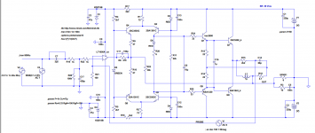
Apparently I had nothing better to do, so inspired by recent renewed interest in current dumping amps, it was only natural, to come up with LMK-style current dump amp. What's more 'unusual' than that?
I have two schematics, one better and one, as we can guess - worse.
The better (in a relative way) one is based on the OS from current-dumping-class-performance-idle-current thread
designed by jxdking.
It has a local feedback within the OS, and global feedback to the op-amp.
Wonder if there is a way to improve on it?
Attachments
Last edited:
variations
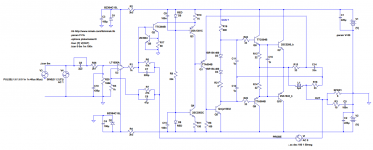
Lots of interesting ideas! I actually like the bjt version better, mostly because the other VAS is running so hot. A P-P VAS could run half as much current. But maybe you could run ~C14 back to Q2 and Q3? You have me investigating the whole issue of nested feedback loops and I like to put the inner loop around the op-amp instead of around the discrete stages. It seems to fix a phase margin issue at lower frequencies. Years ago, I fought with Phase Linear amps that used an op-amp and were notoriously unstable. At the time my best solution was to add local feedback around the op-amp. I'm sure this compromises THD but stability was more important to me. I also don't like lead caps in the global feedback, since that creates a RFI vulnerability, RF on the speaker cables getting to the (fast) front end. I found that you don't need them if you put a ~1nF cap on the emitter of the first transistor and a larger resistor to -8V*, which also limits the current, no need for clamping.
Some of this is illustrated in the attached files. *You will also note that I reduced the op-amp supply to ~+-8V since more just exacerbates rail sticking.
Attachments
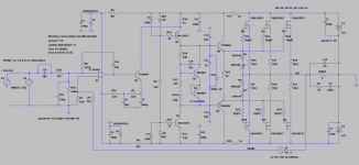
#1021 ????????????? ????????? ?? ????????? ??????????? 1977- 2021 (?????? ? ??????????) - ???????? 52
Top left corner.
Last edited:
Russian web site
Some times my browser offers to translate and some times it doesn't.
So I grabbed the Micro-Cap *.cir file. Microcap is now free and I use it to view *.cir files. But you get an error that is just the Russian file name. So I renamed it using "yM BB 34.cir" instead of the Cyrillic characters and now Micro-Cap will load it.
I note that this amp also has the huge S-curve phase response. This worries me and seems like there is almost no phase margin at lower (~50KHz) frequencies. I think the standard stability criteria assumes that the phase response at 0dB loop gain is the worst case but that is not true in this case.
BTW, the op-amp is AD8065.
Attachments
Last edited:
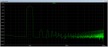
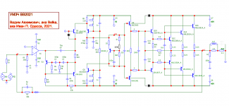
I tried to sim these amps in ltspice, including the same amp Steve tried.
Phase plot is crossing 180 degrees TWICE (or more), which definitely is not acceptable.
These amps are unstable. I built one if them, ignoring S shaped PM, but it was impossible to make it stable. So no more of this for me..
Actually MOST of lmk style amps from that forum is like this, no one seems to mind this kind of Phase plot..
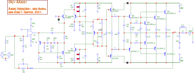
I managed to tweak this amp, so the Phase doesn't cross 180 degrees twice, but it was difficult to lift it ABOVE 180 degrees.
See attached sim in ltspice. THD is very low, FFT profile looks nice,
but Phase plot is still strange, and PM is positive, not negative - Phase crosses 180 degrees way before Gain crosses 0 dB.
And of course once Phase is more or less improved, it's impossible to get square waves in order...
Phase plot is crossing 180 degrees TWICE (or more), which definitely is not acceptable.
These amps are unstable. I built one if them, ignoring S shaped PM, but it was impossible to make it stable. So no more of this for me..
Actually MOST of lmk style amps from that forum is like this, no one seems to mind this kind of Phase plot..
I managed to tweak this amp, so the Phase doesn't cross 180 degrees twice, but it was difficult to lift it ABOVE 180 degrees.
See attached sim in ltspice. THD is very low, FFT profile looks nice,
but Phase plot is still strange, and PM is positive, not negative - Phase crosses 180 degrees way before Gain crosses 0 dB.
And of course once Phase is more or less improved, it's impossible to get square waves in order...
Attachments
Last edited:
- Home
- Amplifiers
- Solid State
- Unusual amp from 1987