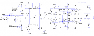
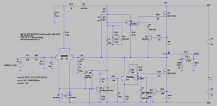
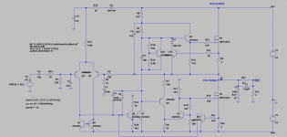
Here is another 'unusual' amp, that I most likely will try to build.
An Apex-style frankenamp that consists of
a) Philips 22AH578 op-amp input stage
b) LMK/Wiederhold style VAS (no need to argue what is and what is not VAS in this case)
c) and excellent Lexan Output Stage by LKA.
All sims look pretty good, it runs B-class cold, and seems to be very stable (PM=65, GM=14) and fast
a) and b) have been already tested together in previous build, and I'm very happy with that amp.
Attachments
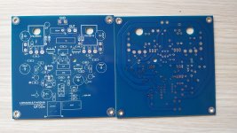
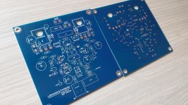
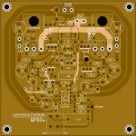
Lomakin & Parshin QF50m PCB
After an unusually long production time, the pcbs finally arrived today. The arrival of the PCb of LMK+Philips hybrid amplifier (Tietze & Schenk BA-50m) is yet to be seen. It was given 'Lomakin & Parshin QF50m' nickname because the original designer of the topology was Lomakin and Parshin, "QF" means QFET output, "50" because it is 50W, and "m" because "minek123" is the designer of this circuit.
After an unusually long production time, the pcbs finally arrived today. The arrival of the PCb of LMK+Philips hybrid amplifier (Tietze & Schenk BA-50m) is yet to be seen. It was given 'Lomakin & Parshin QF50m' nickname because the original designer of the topology was Lomakin and Parshin, "QF" means QFET output, "50" because it is 50W, and "m" because "minek123" is the designer of this circuit.
Attachments
Last edited:
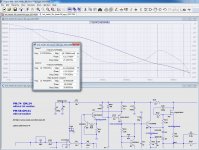
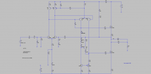
Features of "downscaled" (36V) version:
• Protection transistor to current mirror/driver transistor added (suggested by steveu)
• GD snubber to output FETs added. However it affects the stability noticeably. See above.
• Q7 replaced from TTC004B to 2SC3503C, the latter has 4 times lower Cob and ensures better stability.
• Source resistors omitted, according to Bob Cordell if we have supply rails no more than 50V and Iq no more than 300mA we can do that (using single pair of FETs and assuming good thermal tracking) We will see.
• RC/RL network to output added and optimized
• Input low pass filter and feedback network slightly modified. Phase shift @20kHz is 5.8° now.
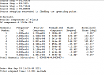
• Compensation modified. Stability margins: PM 74° GM 24dB without and PM 58° GM 31dB with GD snubber.
Pic 4: THD at full power, before clipping 1kHz, 6ohm
• Protection transistor to current mirror/driver transistor added (suggested by steveu)
• GD snubber to output FETs added. However it affects the stability noticeably. See above.
• Q7 replaced from TTC004B to 2SC3503C, the latter has 4 times lower Cob and ensures better stability.
• Source resistors omitted, according to Bob Cordell if we have supply rails no more than 50V and Iq no more than 300mA we can do that (using single pair of FETs and assuming good thermal tracking) We will see.
• RC/RL network to output added and optimized
• Input low pass filter and feedback network slightly modified. Phase shift @20kHz is 5.8° now.
• Compensation modified. Stability margins: PM 74° GM 24dB without and PM 58° GM 31dB with GD snubber.
Pic 4: THD at full power, before clipping 1kHz, 6ohm
Attachments

Last edited:
After an unusually long production time, the pcbs finally arrived today. The arrival of the PCb of LMK+Philips hybrid amplifier (Tietze & Schenk BA-50m) is yet to be seen. It was given 'Lomakin & Parshin QF50m' nickname because the original designer of the topology was Lomakin and Parshin, "QF" means QFET output, "50" because it is 50W, and "m" because "minek123" is the designer of this circuit.
Egra, as usual - beautiful board! Your collection of amps slowly grows 🙂
>Compensation modified. Stability margins: PM 74° GM 24dB without and PM 58° GM 31dB with GD snubber.
Very impressive numbers.
How did you select/calculate snubber's values?
Very impressive numbers.
How did you select/calculate snubber's values?
Thank you Minek, as usual - excellent circuit! I learn more and more day by day, I'm trying to do the best I can.
How did you select/calculate snubber's values?
Choosed values are based on Hugh’s suggestion. In his view, the values are not so critical
Last edited:
Do you have oscilloscope now?
I remember while ago, when you were building Bloomley amp, you mentioned that you didn't have one...
I remember while ago, when you were building Bloomley amp, you mentioned that you didn't have one...
I ordered a digital scope from ebay plus 100W 8 and 4 ohms dummy loads. It’s not okay to go to colleagues or friends to measure my newest amplifiers. You're right DMM is no longer enough.
With bandwidth 0-200kHz you are not going to see any higher frequency oscillations typical for Fets, so we won't know if the snubbers are working correctly 🙂
For this price, it's a great deal. This will be enough for tuning square waves response, crossover distortion, and testing clipping.
For this price, it's a great deal. This will be enough for tuning square waves response, crossover distortion, and testing clipping.
Last edited:
With bandwidth 0-200kHz you are not going to see any higher frequency oscillations typical for Fets, so we won't know if the snubbers are working correctly 🙂
For this price, it's a great deal. This will be enough for tuning square waves response, crossover distortion, and testing clipping.
Yes, I know. But it was dirty cheap and I spent to much money at mouser last weeks. Maybe it will be suitable for a start. I think this will be the next one: 1014D 7" Digital Oscilloscope TFT-LCD Display Professional Oscilloscope
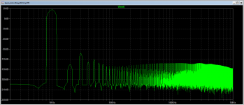
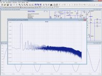
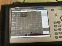
Sometimes even a 100MHz oscilloscope doesn't help and you have to use a spectrum analyzer. The picture shows the oscillation of the VAS (EF + Hawksford cascode) at 20kHz sine, near clipping.
Attachments
Last edited:
Ladislav, what do you think about
the amp from post #1641 with your Lexan OS?
Do you think it is good idea to build it?
the amp from post #1641 with your Lexan OS?
Do you think it is good idea to build it?
Hard to say 🙂 I use it as a buffer now. With global feedback it had some problems when high loopgain front-end was used (even though in simulator had not). Maybe Class-G extension cause the problems, I Dunno.
N Latfet Amp
Here is new amp - the goal was to:
1) have op-amp input, in a spirit of all these amps in this thread
2) all N output devices - but not quasi
I was inspired by Elvee's Circlophone, and several articles from (as usual) Russian Radio magazine (E.g. issue 1980-03), and Quasi's ACTRK600.
I was initially working on the HexFet version - which is still work in progress.
It shows great sim numbers, but for some strange it's slow (10V/us). Not sure why.
So I'm currently working on making it faster. Will publish it later on.
In a meantime - Latfet version is much simpler and easier, and it can nicely illustrate the idea.
Double-die Exicon N latfets are used here.
It only employs 4 small transistors, one TO-126, and 2 output devices, so it's a very spartan amp (not counting op-amp).
It's stable (Phase Margin: 47, Gain Margin: 12), and should be very easy to build.
Slew rate seems to be at least 66V/us.
Any comments and ideas for improvement?
Attachments
-
namp_latfet.18oct.3.asc9.6 KB · Views: 119
-
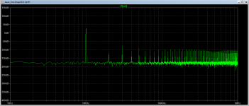
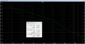 namp_latfet.18oct.3.olg.png52.7 KB · Views: 249
 -
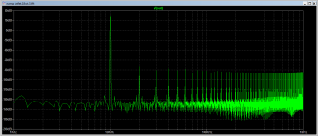 namp_latfet.18oct.3.10khz_fft.png26.1 KB · Views: 183
 -
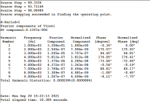
 namp_latfet.18oct.3.10khz_thd.png16.2 KB · Views: 319
 -
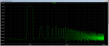 namp_latfet.18oct.3.1khz_fft.png26.5 KB · Views: 315
 -
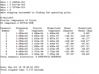 namp_latfet.18oct.3.1khz_thd.png16.1 KB · Views: 395
 -
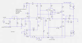 namp_latfet.18oct.3.png36 KB · Views: 406
Last edited:
Quasi NMOS
I'm not a fan of Circlophone circuits because the feedback loop around the lower NPN/NMOS is a long route and bias is tricky. I have played with some Quasi-VNMOS circuits and one is similar to "namp.." but I ended up adding a pnp making it sort of quasi in order to fix some ~clipping issues. Q10 in "namp.." is actually positive feedback and THD is a bit better if you just ground the base. Using latfets means the Vto is very low which then means that pull-down resistors need to be small for slew rate but then you need lots of driver current for good gate on-voltage... I feel that Quasi circuits in 2021 are not worth the trouble but here are a couple anyway. These do not have spectacular THD but at about 0.01% I become more interested in stability and efficiency. Note that QMOS6 is essentially class-B and still gets fair THD.
I'm not a fan of Circlophone circuits because the feedback loop around the lower NPN/NMOS is a long route and bias is tricky. I have played with some Quasi-VNMOS circuits and one is similar to "namp.." but I ended up adding a pnp making it sort of quasi in order to fix some ~clipping issues. Q10 in "namp.." is actually positive feedback and THD is a bit better if you just ground the base. Using latfets means the Vto is very low which then means that pull-down resistors need to be small for slew rate but then you need lots of driver current for good gate on-voltage... I feel that Quasi circuits in 2021 are not worth the trouble but here are a couple anyway. These do not have spectacular THD but at about 0.01% I become more interested in stability and efficiency. Note that QMOS6 is essentially class-B and still gets fair THD.
Attachments
Last edited:
>Q10 in "namp.." is actually positive feedback and THD is a bit better if you just ground the base.
I tried that, but it wasn't any better.
> I feel that Quasi circuits in 2021 are not worth the trouble
Right, I gave up on them, it's too much trouble, but I have some hopes for this 'all N' topology. I have a lot of N Hexfets, and they have to go..
It sims as good as complementary OS. As for Hexfet version - as you said - bias (and thermal comp) is tricky..
Last edited:
Steve, in the 2nd schematic (post # 1657) Q9 acts as a temperature sensor and bias generator, is that right?
Q9 is a typical quasi driver and the bias is just the diodes including a led. A VBE multiplier might be better. A degenerated Q9 provides the best XO driver being driven by the same point as the upper gate, but you have to block any reverse collector current so that Q5 can pull the lower gate above the drain/output in order to clip near the negative rail. So, you have two drivers for the lower FET, the PNP at crossover, and Q5 as you get close to clipping. R10 is chosen so that the lower gate voltage does not sag too far from the FET turn on voltage because it takes time to rise.Steve, in the 2nd schematic (post # 1657) Q9 acts as a temperature sensor and bias generator, is that right?
I found a better arrangement of the first circuit that does a couple things better. By wiring Q5 as a VBE multiplier from VDD, you get a controlled gate voltage and limited gain that improves stability. See attached.
Attachments
Hi minek123,....
It shows great sim numbers, but for some strange it's slow (10V/us). Not sure why.
....
Any comments and ideas for improvement?
The circuit you show in post #1655 drives the output LATFETS with just about 1mA through Q4/Q8 and that's unrealistic - you need about 10 mA to successfully drive the gates of a pair of double-die LATFETs. So, in order to accomplish this, you either increase the current through Q4/Q8 or (even better) introduce EF stage between Q4/Q8 and M1/M7 .
Hi steveu..I feel that Quasi circuits in 2021 are not worth the trouble ....
neither Circlophone nor Minek's circuit in post #1655 are quasi-complementary topologies - the output stage transistors are driven with counter-phase signals (similar to circlotron topology or Nelson Pass' FirstWatt F6 amp) so there's nothing "quasi" about them.
- Home
- Amplifiers
- Solid State
- Unusual amp from 1987