Alright. So, a couple of breakthroughs.
1. (and this has to forever stay between us, Mooly; promise?...) It's the second time the protection circuitry has (splendidly!) tricked me. Once removed (one leg of diodes, and all main connecting transistors), I am able to adjust bias, DC offset is reasonable, Vbes all look good. Oh, boy.
2. In terms of "attenuating" circumstances (I will scrape excuses from anywhere I can, alright?), the protection circuitry is a ***HOT*** mess. I don't know how many hands have been on this, and how many times this guy was passed from hand to hand on ePay and elsewhere (probably rendered "un-repairable" by a buncha people), but there's everything from broken traces (which I've seen before, and tested ok, and cleaned up and all, but to make a point) to misplaced transistors (the amp overall has a dizzyingly wide variety of transistors used in misc places, but in the protection circuitry, all that goes to yet another level) and by misplaced, I mean, their legs wrongly connected, no trace of intentionality to keep the channels at least somewhat similar, and stuff like that. Some were failed, some strangely survived. Again, I've seen the "melting pot" of parts being used before, but now under scrutiny I realize what hack job a bunch of people (or maybe one extremely capable one) have done at this.
So, in a nutshell, I think I'll rebuild the protection circuitry with new parts entirely (Qs, I mean), and then fire it up and see if the full functionality of the actual amp I seem to observe now maintains.
Before that though, and though a bit apprehensive about this, I will maybe keep volume pots at 1W level and check if a sine passes OK through it. This way I'd know this is it.
A couple of preliminary learning points:
- Never assume whoever previously worked on the thing you're working on did a decent job. Check things at a high level. Channels very dissimilar in terms of parts used? All transistors matching their pin configuration? Soldering job OK? Broken traces? Sings of abuse anywhere? Negligently missing screws?...
- In troubleshooting, if things are confusing/make little sense, hook up a bulb test fixture and disable the protection circuitry. Having a "naked" amp, you can much more easily see what's working as you're evaluating and assessing typically pretty simple circuitry.
")
I wonder... there was a recent thread with problems with the protection circuitry not closing the speaker relay:
Sony TA-3650 power rail resistors burn
and we were looking at the relay circuit in isolation. The DC offset values as applied to the board were good, and all the voltage readings on and around the board were good and yet the relay wouldn't activate and close. Thoughts of low gain transistors... all sorts were considered.
Finally we used a scope to check the DC values rather than a DVM and then it all became clear and the puzzle fitted together.
The 'fault' causing the relay not to close was a blown fuse elsewhere in the amp and the relay board was missing one of a full wave AC input to detect the presence of 'power on' and that caused excess ripple on a few critical points, enough to hold some of the transistors in the relay driver off.
So all the DC voltages were appearing correct with a DVM, but a scope showed the problem.
Never assume... and that in a way is where the above went wrong. I always say to check rails as a first step and yet the relay board was self contained and only needed supply, AC detection and DC offset inputs to work. And on a DVM all were good. What we didn't check was the DC supplies elsewhere... why would we when all the voltages on the relay section were correct
Agreed - sometimes you get curve balls and the answer you need is two scenarios over out of focus. In my case, I got the same curve ball twice but still failed to see it 
Now on to the PC rebuild. I'm going to go generic 2N5401/2N5550 most everywhere. On the diodes, I'm checking as I go, but one that's a bit puzzling is the D110/111 pair. It seems they just need to drop 0.6V (vanilla junction). Why then have they used a different diode - SH-1S vs. IT243M. I'd clean all that up and just use a couple of 1N4148s, but I'm hesitating as I don't really get the part difference.
Now on to the PC rebuild. I'm going to go generic 2N5401/2N5550 most everywhere. On the diodes, I'm checking as I go, but one that's a bit puzzling is the D110/111 pair. It seems they just need to drop 0.6V (vanilla junction). Why then have they used a different diode - SH-1S vs. IT243M. I'd clean all that up and just use a couple of 1N4148s, but I'm hesitating as I don't really get the part difference.
D111 is a Zener but don't ask me what voltage, D110 I would guess just a small signal type although I don't know what current it might see under overload conditions.
You could check the other channels diode in a simple test circuit... 9 v battery and resistor and see what voltage it is. If 9v isn't high enough then tag a resistor and the Zener across a rail. Limit the current to around 5 milliamps, so around 12k.
You could check the other channels diode in a simple test circuit... 9 v battery and resistor and see what voltage it is. If 9v isn't high enough then tag a resistor and the Zener across a rail. Limit the current to around 5 milliamps, so around 12k.
Alright. after rebuilding the Q107/108/109/114 & Co protection circuitry I fired it again and I went a bit more confidently and thorough on the adjustments. Bias is pretty solidly on 25mV, and DC offset is less than a mV, both channels.
Basically, what I'm doing is reconnecting the protections one by one so I track where things go riot. Chances are all my issues were due to the messed up PC (above) that I just rebuilt.
I have not yet passed signal through, though I can't imagine I will not get to that point tonight (Pacific time).
The D110/111 & Co protection I regard as very secondary; I may just run it with it disconnected. Thank you for your detailed thoughts above, I was able to find some indication of the mechanism there in the manual too. Sources online quote between 7.2V and 9.1V, depending who you read... Will measure it though and for sure pot here for others to not have to go through it.
Basically, what I'm doing is reconnecting the protections one by one so I track where things go riot. Chances are all my issues were due to the messed up PC (above) that I just rebuilt.
I have not yet passed signal through, though I can't imagine I will not get to that point tonight (Pacific time).
The D110/111 & Co protection I regard as very secondary; I may just run it with it disconnected. Thank you for your detailed thoughts above, I was able to find some indication of the mechanism there in the manual too. Sources online quote between 7.2V and 9.1V, depending who you read...
Will measure it though and for sure pot here for others to not have to go through it.Well, the "2nd PC" (Q303-307) shut it down again, so I had to dive into it. Q306 was leaky C-E and B came right off with the desoldering pump... I guess being always on kept the power limiter in an ON status of sorts.
In a nutshell, two different protection circuits were acting up and likely fighting each other at that. This, aside from the bad CCS and one side of the LTP... A lot going on, overall. Some may have been triggered by my testing of it, but the other conditions only flipped it over the edge on some of the issues. I probe with heatshrink on the tip of the probe, so only the tippy tip gets exposed and makes contact.
Anyway, Q306 is an 2SC1124. The best candidates I could find at hand were the same MJE340 (though it can only handle 0.5A Ic), and 2N3440 (which can handle 1A Ic, but, depending how you look, either dissipates 1W or 10W...). I don't think this will ever handle much - if ever used - so I decided to use the 2N3440 - would be interested in thoughts on my choice.
The only real thing left for tonight is figuring out the 1T243 voltage. Music is tomorrow, got a 6 year old that's just about to fall asleep.
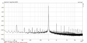
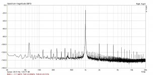
I enclose some quick measurements. Interesting thing is - the R channel is all new, current production Qs on the input, and has distinctly lower distortion numbers. Having said that, the old one also had a channel with much lower distortion readings, also R, so take that with a grain of salt.
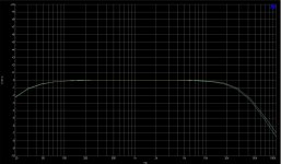
The frequency response is not as good as the old one's at the high end... Not entirely sure why. I am considering replacing the low value ceramic caps - which look very bad, all sorts of oxide and deposits on them - with C0Gs and polys where I can, see if that makes a difference.
Anyway, pretty happy camper tonight. Thank you VERY MUCH for helping with all this, Mooly.
In a nutshell, two different protection circuits were acting up and likely fighting each other at that. This, aside from the bad CCS and one side of the LTP... A lot going on, overall. Some may have been triggered by my testing of it, but the other conditions only flipped it over the edge on some of the issues. I probe with heatshrink on the tip of the probe, so only the tippy tip gets exposed and makes contact.
Anyway, Q306 is an 2SC1124. The best candidates I could find at hand were the same MJE340 (though it can only handle 0.5A Ic), and 2N3440 (which can handle 1A Ic, but, depending how you look, either dissipates 1W or 10W...). I don't think this will ever handle much - if ever used - so I decided to use the 2N3440 - would be interested in thoughts on my choice.
The only real thing left for tonight is figuring out the 1T243 voltage. Music is tomorrow, got a 6 year old that's just about to fall asleep.
I enclose some quick measurements. Interesting thing is - the R channel is all new, current production Qs on the input, and has distinctly lower distortion numbers. Having said that, the old one also had a channel with much lower distortion readings, also R, so take that with a grain of salt.
The frequency response is not as good as the old one's at the high end... Not entirely sure why. I am considering replacing the low value ceramic caps - which look very bad, all sorts of oxide and deposits on them - with C0Gs and polys where I can, see if that makes a difference.
Anyway, pretty happy camper tonight. Thank you VERY MUCH for helping with all this, Mooly.
Attachments
Sounds like you are making real progress now Those transistors in the protection circuitry will never see much current at all.
Q306 appears to simply shunt the two driver transistor bases together via two series diodes D312 and D316 etc. That reduces the bias to zero but has no other impact on power output.
It would reduce dissipation at high frequencies and high output levels where cross conduction of the output stage could occur.
The transistor and diodes see only a couple of milliamps at most.
Q304 and Q305 also operate in a similar way but these clamp the drive voltages independently (plus half and neg half) to ground. These can see a bit more current, up to around 30 milliamps for the negative clamp, and considerably less for the positive side.
I've tried both in the simulation.
So its getting there
Those transistors in the protection circuitry will never see much current at all.Q306 appears to simply shunt the two driver transistor bases together via two series diodes D312 and D316 etc. That reduces the bias to zero but has no other impact on power output.
It would reduce dissipation at high frequencies and high output levels where cross conduction of the output stage could occur.
The transistor and diodes see only a couple of milliamps at most.
Q304 and Q305 also operate in a similar way but these clamp the drive voltages independently (plus half and neg half) to ground. These can see a bit more current, up to around 30 milliamps for the negative clamp, and considerably less for the positive side.
I've tried both in the simulation.
So its getting there
Music from this point on. And it does indeed sound great.
I ended up using one of those 6.8V zeners (1N5235B), and added a forwarded biased vanilla junction (1N914B), ending up with the exact same voltage to the third digit after the comma. I didn't expect this, but I had to readjust everything (not a matter of warm-up). BTW - this was another dissimilarity between channels, D210 used an old, very thick legs (maybe 1W?) GE zener doing 12V. Filed in the "tech(s) messing up" category.
I ended up using one of those 6.8V zeners (1N5235B), and added a forwarded biased vanilla junction (1N914B), ending up with the exact same voltage to the third digit after the comma. I didn't expect this, but I had to readjust everything (not a matter of warm-up). BTW - this was another dissimilarity between channels, D210 used an old, very thick legs (maybe 1W?) GE zener doing 12V. Filed in the "tech(s) messing up" category.
- Status
- This old topic is closed. If you want to reopen this topic, contact a moderator using the "Report Post" button.
- Home
- Amplifiers
- Solid State
- Sony TA-3200F: huge output DC offset