

Must have done something wrong somewhere assembling the 4 ohms version... On initial powerup i'm getting 20Vdc offset... No smoke nothing though...
Noticing that on v131, I'm using BD140-16 which has a different gain range than BD140... Don't know if that could crap it out...
In the meantime, I'll keep searching... If you have any hints, it would be appreciated.
Do
Noticing that on v131, I'm using BD140-16 which has a different gain range than BD140... Don't know if that could crap it out...
In the meantime, I'll keep searching... If you have any hints, it would be appreciated.
Do
Hi Do,
When the amp doesn’t draw normal Class A bias current, something is amiss with the circuitry driving the gate of the CCS. You are correct to look at the BD140 but I don’t think the gain really matters that much. I think I actually used a KSA992 there. If using flying leads for the outputs, are the wires all correct?
When the amp doesn’t draw normal Class A bias current, something is amiss with the circuitry driving the gate of the CCS. You are correct to look at the BD140 but I don’t think the gain really matters that much. I think I actually used a KSA992 there. If using flying leads for the outputs, are the wires all correct?
Last edited:


ok, checked a few things... First was to clean the underside of the PCB, just in case there was a bead of solder somewhere causing a short... But it didn't make a difference. Well... my PCB is all clean! ")
V113 is reading 1V, but switching leads polarity on BE, then reads .780V
I replaced the KSC3503DS just in case but it was good... Same voltages after changing it. Also changed V131 for KSA992 (checked pinout), as X is using it on his build, but since there's not enough voltage to turn it on, it doesn't make any difference...
Checked all resistors from the 4 ohms build and they all match.
My input voltage rails are +/-23Vdc, because it's the 4 ohms build.
Any more things I should check?
Again, thanks for your help!
Do
Hi Hugh,
Here's a few measurements, some might not be helpful at all, but I've included them anyways...
N Channel side (FQA40N25) - Measurements are all referenced to 0v (PSU ground)
Ground to Drain = 23.39V
Ground to Gate = -17.16V
Ground to Source = -20V
These measurement are taken with positive lead on Drain
Drain to Source = 43.29V
Drain to Gate = 42.45V
P Channel side (FQA36P15) - Measurements are all referenced to 0v (PSU ground)
Ground to Drain = -23.31V
Ground to Gate = -23.15V
Ground to Source = -20V
These measurement are taken with positive lead on Drain
Drain to Source = -3.13V
Drain to Gate = 0V
DC Offset = -20V
Hope this helps in helping me
Thanks
Do
Hi Do,
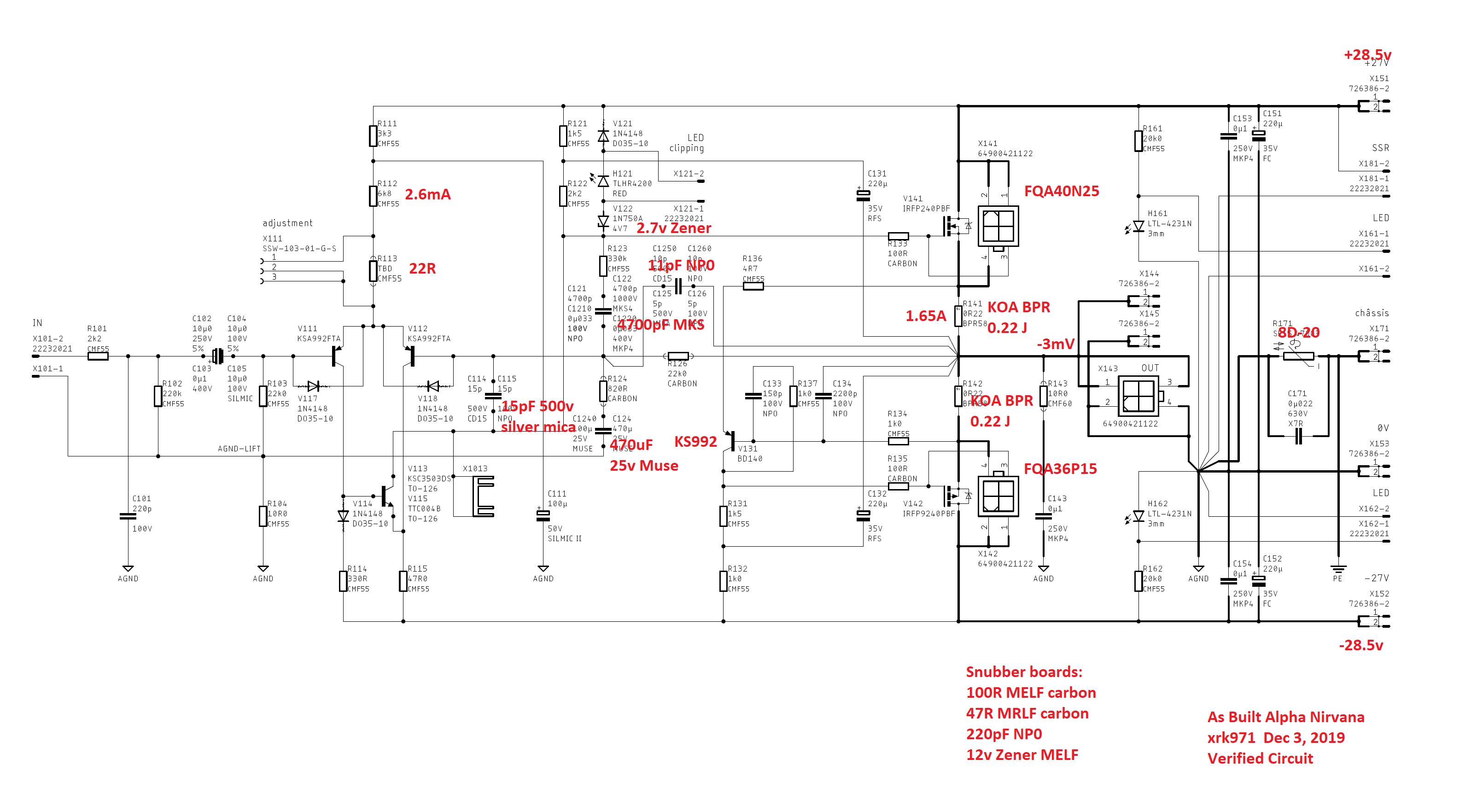
If we look at the DC setpoints of the LTSpice simulation (and I know it’s for 8ohm version but the 4ohm won’t be far off with respect to voltages at the pins of MOSFETs).
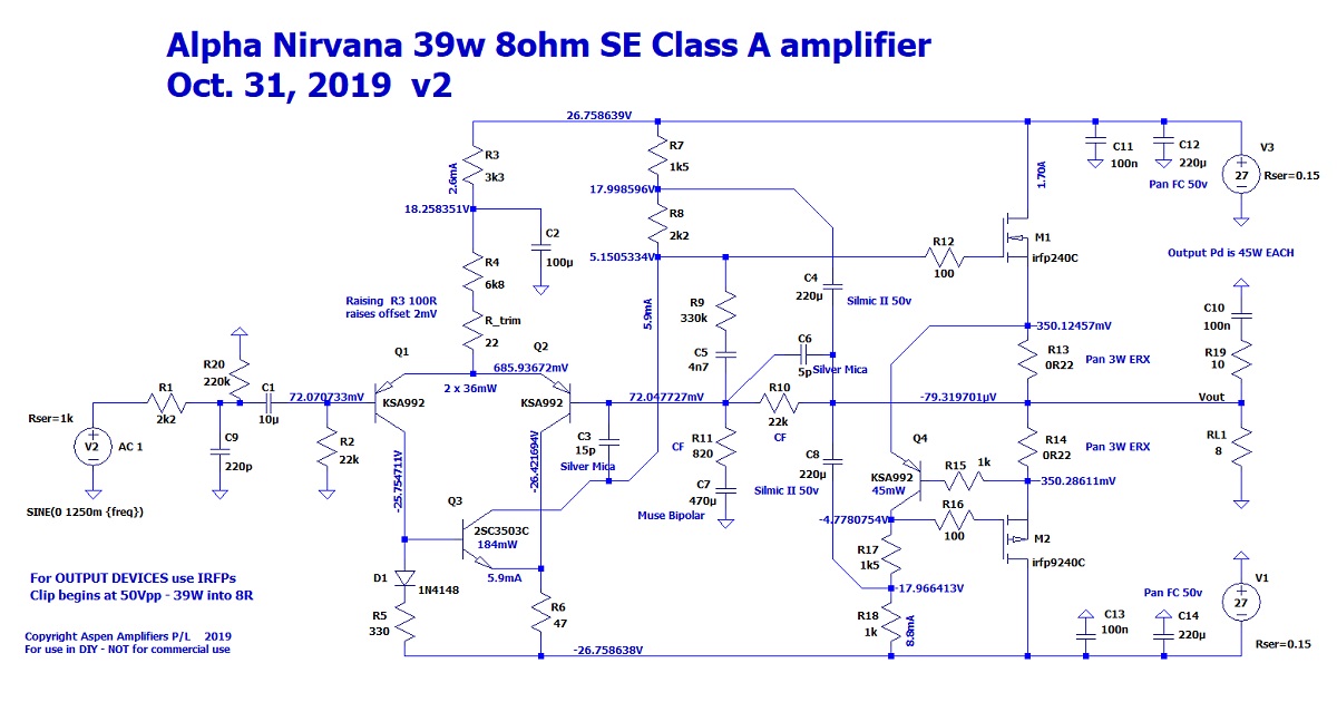
Look at the gate voltages at the MOSFETs. For the N ch it’s about +ve 4-5v and for P ch it’s about -ve 4-5v.
Your probe measurements show something is not turning on the P channel so there is no current flow. Your P ch gate is about the same as the negative rail. For that to happen it means that there is no current flowing through the KSA992/BD140, thus the voltage at the collector will equilibriate to the negative rail that it is attached to through the resistors. A similar thing can happen if the KSC3503 is not flowing any current. The voltage at the gate of the N ch is this negative when it should be about 5v.
So check for cold solder joints on the KSC3503 (Q3 above), and KSA992 (Q4 above). These are robust BJTs. I have hardly ever had one go bad. If resistors are good and BJTs are correct and pin outs are correct, then it can only be a bad or cold solder joint, or a bad electrolytic cap that has shorted. Check the bootstrap caps (C4 and C8 above) to make sure they are not bad, or shorted.
Can you post voltages on pins at Q3?
If we look at the DC setpoints of the LTSpice simulation (and I know it’s for 8ohm version but the 4ohm won’t be far off with respect to voltages at the pins of MOSFETs).
Look at the gate voltages at the MOSFETs. For the N ch it’s about +ve 4-5v and for P ch it’s about -ve 4-5v.
Your probe measurements show something is not turning on the P channel so there is no current flow. Your P ch gate is about the same as the negative rail. For that to happen it means that there is no current flowing through the KSA992/BD140, thus the voltage at the collector will equilibriate to the negative rail that it is attached to through the resistors. A similar thing can happen if the KSC3503 is not flowing any current. The voltage at the gate of the N ch is this negative when it should be about 5v.
So check for cold solder joints on the KSC3503 (Q3 above), and KSA992 (Q4 above). These are robust BJTs. I have hardly ever had one go bad. If resistors are good and BJTs are correct and pin outs are correct, then it can only be a bad or cold solder joint, or a bad electrolytic cap that has shorted. Check the bootstrap caps (C4 and C8 above) to make sure they are not bad, or shorted.
Can you post voltages on pins at Q3?
Last edited:

- Home
- Amplifiers
- Solid State
- Alpha Nirvana 39w 8ohm Class A Amp