This:
https://www.mouser.ch/ProductDetail...1JkyatAb/wA==&countrycode=CH¤cycode=CHF
Reading the specs it should have the same characteristics as the one specified in the USSA BOM. It has a nice lug mount to fix it on the heatsink, which I need for my "off-PCB" installation.
https://www.mouser.ch/ProductDetail...1JkyatAb/wA==&countrycode=CH¤cycode=CHF
Reading the specs it should have the same characteristics as the one specified in the USSA BOM. It has a nice lug mount to fix it on the heatsink, which I need for my "off-PCB" installation.
Hi Mbrennwa
Your GND tab (input/feedback gnd) close to V- is not Connected. You are using the power ground which has no effect at this stage of the build. If that is the case then you have floating ground on pcb.
The manual says “Connect V+ and V- and PGND (the one close to V-) to power supply (from 15Vdc to 30Vdc).” The original pcb had 2 times PGND tabs which was corrected in subsequent pcb versions. Unfortunately the manual was not modified to include the new corrected pcb designation, sorry. In any case, as a general statement, I am indicating the minimum gnd scheme based on the build step but if you always connect both ground tabs to PSU it will always work at any step of the build.
Fab
Last edited:
Oh no, more grounding confusion... the other build steps are very specific about which (P)GND terminal should be used (see for instance 8.7, which explicitly states both GND and PGND). I therefore assumed that step 8.14 is specifically meant to use PGND only.
Anyway, I joined the GND and PGND terminals, but that didn't help for step 8.14. I still get the same issue as before.
Looking at the schematic and trying to understand the purpose of the adjustments described in 8.14, I actually think the node where the two driver MOSFETS M3 and M4 are joined together needs to be grounded for the adjustment procedure described in 8.14. Otherwise, the potential at this node will wander up and down along with the P1 adjustment, upsetting the P2 setting (and vice versa). I tried grounding the the OUT terminal to GND, and tadaaa! I could adjust the voltages just fine as described in step 8.14. Fab, can you please check this and confirm if this is right or not!?
Oh, before anyone takes a close look at my boards and starts wondering:
- C5 and C6 are on the back of the board
- The gate resistors R17, R18, R19, R20 and the diodes D1, D2, D3, D4 are on the pins of the MOSFETs, not on the board. The board has jumper wires in place of the gate resistors.
Hi Mbrennwa
If you look at figure 18 for this procedure step, OUT is referenced to ground - 8 ohms is almost like ground for this adjustment. Maybe I should have pointed that out in the text too. I can add it in a next manual version. Sometimes it can also work without OUT to ground but this might be luck.
I am still worried about your wire length going to transistors and thermistors....🙄
This is a very low feedback design with big margin on frequency compensation but if it was otherwise I doubt it would work with that long wires arrangement. I suppose that you will shorten these wire length in the final build as much as possible.
Fab
Last edited:
Ok, I see, you assumed that readers would (1) actually look at the figure and (2) discover the 8R at the output. Didn't work for me. The manual text is written with very detailed step-by-step instructions, but no mention of the 8R to GND. I didn't realise you wanted the OUT terminal connected to GND (via the 8R) for step 8.14.
In any case, I believe I'll just stop following the step-by-step instructions, as they don't seem to work very well for me. I believe I understand the schematic, and I'll just take it from there. All I needed to extract from the text are the targeted bias points for the input, driver and output stage. Adjusting the pots and the load resistors for the drivers should be straight forward from this.
So far, here's how I think biasing should work pretty easily:
- Input stage CCS bias current: set to 2.8 mA (28 mV across R11 and R12, adjustment by P3 and P4)
- Driver MOSFET bias current (M3 and M4): set to 23 mA (adjustment by tweaking the RV1 and RV2 values)
- Output MOSFETS bias current (M1 and M2): set to 1 A (adjustment by P1 and P2), can be biased higher if heatsinks and PSU are happy
- Output DC is adjusted by adjusting P1 and P2
- Note: the ratio of P1 / P2 controls OUT DC, the absolute P1 and P2 values control output bias current.
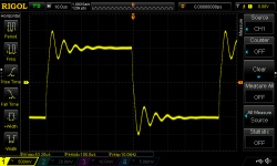
I know that the leads between the board and the MOSFETs are longer than one would like. The photos just show the bench-test setup, and it has gone way more spaghetti since I took those shots. Nevertheless, the scope does not show any traces of oscillation. Also, I will of course shorten and tidy up the leads in the final build.
In any case, I believe I'll just stop following the step-by-step instructions, as they don't seem to work very well for me. I believe I understand the schematic, and I'll just take it from there. All I needed to extract from the text are the targeted bias points for the input, driver and output stage. Adjusting the pots and the load resistors for the drivers should be straight forward from this.
So far, here's how I think biasing should work pretty easily:
- Input stage CCS bias current: set to 2.8 mA (28 mV across R11 and R12, adjustment by P3 and P4)
- Driver MOSFET bias current (M3 and M4): set to 23 mA (adjustment by tweaking the RV1 and RV2 values)
- Output MOSFETS bias current (M1 and M2): set to 1 A (adjustment by P1 and P2), can be biased higher if heatsinks and PSU are happy
- Output DC is adjusted by adjusting P1 and P2
- Note: the ratio of P1 / P2 controls OUT DC, the absolute P1 and P2 values control output bias current.
I know that the leads between the board and the MOSFETs are longer than one would like. The photos just show the bench-test setup, and it has gone way more spaghetti since I took those shots. Nevertheless, the scope does not show any traces of oscillation. Also, I will of course shorten and tidy up the leads in the final build.
Thermistors
I too prefer the lug type but did not pursue this option because one of the members here had an issue when setting the bias.
Good luck with that and the long wire lengths.
I too prefer the lug type but did not pursue this option because one of the members here had an issue when setting the bias.
Good luck with that and the long wire lengths.
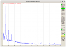
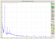
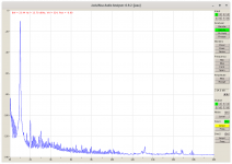
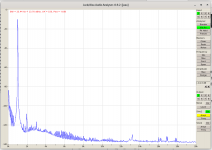
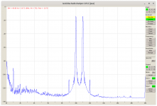
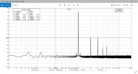
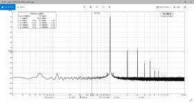
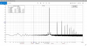
Here are some measurements from the test setup as shown in post 1500 (dummy heatsink with lots of spaghetti). Bias points were adjusted as described in post 1506. The amp was running on +/- 25 VDC from cheap lab-bench PSUs. Measurements were done at 1 Vrms into a 4 Ohm load. The output bias was set to 0.7 A, 1.0 A, 1.5 and 2.0 A (IMD was measured at 1.0 A only).
Not surprisingly, higher bias gives lower harmonic distortion. THD is very low overall, and harmonics show a very nice decay with 2nd higher than 3rd (and higher harmonics are below noise floor).
Looks good to me! Thanks Fab for this nice amp!
P.S.: The output DC is rock steady within single-digit millivolt range if heatsink temperature changes. The temperaure compensation works perfectly with the lugged thermistor part!
Attachments
You are welcome Mbrennwa!
I start my own THD measurement at 1Wrms but your measurement appears consistent with mine so it is excellent at this stage. 🙂
Note that the possible long wires effect should normally not show on such THD measurement. Only 10KHz square wave with RC load and check with scope will normally reveal for sure such an issue - if it is really the case of course. I see other amplifiers using a correction network close to the output mosfet to “patch” this potential issue. If you can manage to have it worked without it then it means my amp is really permissible to long wires...😉
I am anxious to see your integration of the amp into your nice chassis and get your feedback on the sound 🙂
Keep on the good work!
Fab
P.S. I am taking note on your comments for a next version of the build manual.
Last edited:

This seems good for 0.82uF.
however I would also check with some values of C from 4nF to about 1.2uF to be sure.
Fab
however I would also check with some values of C from 4nF to about 1.2uF to be sure.
Fab
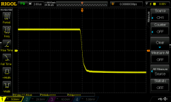
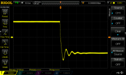
Here are the scope shots for R = 4 Ohm with C = 1 uF, 0.1 uF, 0.01 uF, 0.001 uF and no-cap. Note the different time scales (shown on top left).
Attachments


Your THD graphs look great!
If you have the time/ inclination I would be interested to see a THD test at 1A or 1.5A bias at 1Khz and 10Khz at say 10Watts.
I'm glad the lug thermistor worked out for you.
If you have the time/ inclination I would be interested to see a THD test at 1A or 1.5A bias at 1Khz and 10Khz at say 10Watts.
I'm glad the lug thermistor worked out for you.
Good response to square waves Mbrennwa 
For THD at higher power these are the curves I took earlier this year for USSA 5.1 (which is very similar to original USSA 5).
Included are for 10 to 25Wrms at 1KHz at 1.25A bias. I do not have a low THD generator for 10KHz but being a low feedback factor CFA amp the profile should be quite good.
For 6W and 1Wrms the curves are in the manual where only H2 and H3 are over the noise floor with H2> H3 at lower than about 8 Wrms or so.
Fab
Attachments

Last edited:
I will take proper distortion measurements later, when my build is in the final chassis. I also ordered some better dummy load resistors.


Wow Mbrennwa!
This looks fantastic
It is a remarkable implementation. It may be the smallest 25Wrms/ 8 ohms (or more?) class A amplifier 😉
I really like it a lot🙂 can I use the picture in my next iteration of the build manual ?
Where will be located the input and output connections.
Can you describe a bit your PSU .
Fab
Last edited:
It is a remarkable implementation. It may be the smallest 25Wrms/ 8 ohms (or more?) class A amplifier 😉
Well, my current Aleph is already there (same chassis). However, the Aleph has an external SMPS, only the CLC smoothing is in the chassis. The USSA will have to full PSU inside the chassis.
I really like it a lot🙂 can I use the picture in my next iteration of the build manual ?
Sure! I may have better photos later on.
Where will be located the input and output connections.
On the bottom. The whole thing will have somewhat taller feet than a typical chassis, which allows some room for (angled) connectors.
Can you describe a bit your PSU .
I have not yet tested the PSU. The plan is to use one 500 VA transformer with 4 x 21 VAC secondaries --> two Smooth Like Buttah power supplies (one per channel) --> USSA5 boards
The chassis is quite a bit of work. Lots of drilling and tapping. I already broke two drill bits, and they are stuck in the aluminium... next time I will buy the expenisve drill bits again 🙄 Drilling / tapping must be dead on centered on the fins, so that the hole is inside the fins and will not visible from the outside.
- Home
- Amplifiers
- Solid State
- USSA-5 Build with Review