Fast on connections advise
The problem with fast on connectors is that upon several removals the female connector starts to become somewhat loose. When the connection is not good enough I can clearly see an increase of THD (sometimes about 10dB) and higher level main line voltage artefacts. So as a general advise ensure you have strong and good connection between female and male tab connector everywhere in the amplifier where you have these connections. The same applies for screw terminais of course. This may seem obvious but it is not so visible....🙄
Fab
Speaking of connectors... I ordered the Molex parts from the BOM in the USSA manual, but the crimp pins are missing. I have no clue about the Molex universe... so, which pins should I get to fit in the connector housing and on the PCB connector? A Mouser part number would be great.
Thanks!
I have the housings specified in the USSA BOM, which are a different part number than what you suggested:
https://www.molex.com/molex/products/part-detail/crimp_housings/0022013037
Will your suggested crimp pins work in the housings I already have?
I have the housings specified in the USSA BOM, which are a different part number than what you suggested:
https://www.molex.com/molex/products/part-detail/crimp_housings/0022013037
Will your suggested crimp pins work in the housings I already have?
Finally getting around to my build (stereo chassis).
So which heatsink shall I use?
Option A) Both amplifier modules installed on the underside of a top mounted single flat bottomed 300x300 heatsink (0.29 °C/W) Example
Option B) Two fan assisted heatsinks mounted inside the chassis (Ultra-Fin™, 0.07 °C/W). Example
🙂
So which heatsink shall I use?
Option A) Both amplifier modules installed on the underside of a top mounted single flat bottomed 300x300 heatsink (0.29 °C/W) Example
Option B) Two fan assisted heatsinks mounted inside the chassis (Ultra-Fin™, 0.07 °C/W). Example
🙂
stretchneck,
One of these per side would be a workable option:
https://uk.farnell.com/h-s-marston/96cn-01500-a-200/heat-sink-0-36-c-w/dp/148120
Or if a chassis with the same height, but deeper, two of these heat-sinks per side:
https://uk.farnell.com/fischer-elektronik/sk-47-150-sa/heat-sink-150mm-0-5-c-w/dp/4621906
Little bit taller but within 300mm depth, one per side of the following (probably best option here):
https://uk.farnell.com/fischer-elektronik/sk-56-200-sa/heat-sink-alum-extruded-0-3k-w/dp/1211722
Last edited:
Ask these guys to give you a quotation for their largest heatsink (MF35-151.5).
Tell them that you support Australia in the cricket😀
Conrad Heatsinks - Products
Tell them that you support Australia in the cricket😀
Conrad Heatsinks - Products

Cheers - good suggestions, but I’d like it to try something a bit different for this build. Am wondering if 0.3 of both modules is a bit on the low side though...
stretchneck,
You might find this article useful for planning your chassis and heat-sink orientation:
http://www.thermalsoftware.com/vert_vs_horz_sink.pdf
You might find this article useful for planning your chassis and heat-sink orientation:
http://www.thermalsoftware.com/vert_vs_horz_sink.pdf

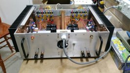
Finally my amp is playing music on my sacrificial speakers.
I've measured 70.5mV on one channel and the other one is at 71mV, across R15 or R16.
Heatsinks are just warm and I can touch the output Mosfets for about 20 seconds. I assume that the heavy copper plate bolted to the heatsink is drawing away most of the heat from the Mosfets.
When I get my speakers out of storage I will do some critical listening. Now to finish off the front panel.
Attachments
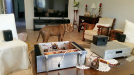
Good stuff Harry3. Looks like man's best friend also likes what he is seeing? Or he's just bored. 🙂
Finally my amp is playing music on my sacrificial speakers.
I've measured 70.5mV on one channel and the other one is at 71mV, across R15 or R16.
Heatsinks are just warm and I can touch the output Mosfets for about 20 seconds. I assume that the heavy copper plate bolted to the heatsink is drawing away most of the heat from the Mosfets.
When I get my speakers out of storage I will do some critical listening. Now to finish off the front panel.
Well done......Harry!!


Hi Fab
Could you post an image of the PCB with the part numbers and the traces/connections in between?
The connections are difficult to see on the PCB, and once the PCB is populated with the parts, the part numbers are not visible anymore. The PCB photo in the manual (Fig. 9) shows the part numbers, but not the traces/connections between the parts. An image with the traces+parts would be useful to understand the connections on the PCB, for instance for debugging purposes etc.
Addendum: I am talking about PCB rev. 0.4
Hi Mbrennwa
I will not post on the forum the pcb layout showing the traces for intellectual property reason where it could be potentially used by a 3rd party for business purpose...😱
Regarding possible debugging activity, the schematics, the parts designation on the pcb and figure 9 should be sufficient. Myself —having done many variations with troubleshooting needs sometimes- do it that way. Also this forum is there to help the builder troubleshooting....😉
Fab

I will not post on the forum the pcb layout showing the traces for intellectual property reason where it could be potentially used by a 3rd party for business purpose...😱
Ok, I see.
Regarding possible debugging activity, the schematics, the parts designation on the pcb and figure 9 should be sufficient.
Sure, I've done it now by having the schematic and the PCB photo next to each other, but it would have been a lot easier and with less potential for screwing up with a PCB image of the traces.
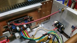
Issues with front end testing
I am running into problems with testing the front end. Step 8.14 in the manual says:
- Adjust P1 for 0.3 V between TP6 and V-
- Adjust P2 for 0.3 V between TP5 and V+
In my build, I can not adjust the voltages independently. If I adjust P1, both voltages will move up and down at the same time. Same with P2. For instance, I could set the voltages to about 0.4 V and 0.2 V. If I adjust P1, I could change the voltages to 0.5 V and 0.3 V (and same for P2). I cannot achieve 0.3 V for both voltages.
This happens with both boards.
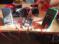
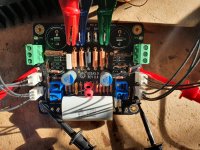
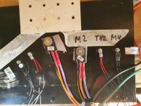
PSU is at +/- 25 VDC (lab / bench supplies). Transistors and thermistors are mounted on a dummy heatsink for testing purposes. Output transistors are not connected to the board. I attached some photos.
Any ideas or suggestions?
I am running into problems with testing the front end. Step 8.14 in the manual says:
- Adjust P1 for 0.3 V between TP6 and V-
- Adjust P2 for 0.3 V between TP5 and V+
In my build, I can not adjust the voltages independently. If I adjust P1, both voltages will move up and down at the same time. Same with P2. For instance, I could set the voltages to about 0.4 V and 0.2 V. If I adjust P1, I could change the voltages to 0.5 V and 0.3 V (and same for P2). I cannot achieve 0.3 V for both voltages.
This happens with both boards.
PSU is at +/- 25 VDC (lab / bench supplies). Transistors and thermistors are mounted on a dummy heatsink for testing purposes. Output transistors are not connected to the board. I attached some photos.
Any ideas or suggestions?
Attachments
- Home
- Amplifiers
- Solid State
- USSA-5 Build with Review