hmm, this looks familiar.
If you change the VAS current mirror for a bootstrap cirucit in swordfish latest schematic, you have a spitting image of rod elliots P101 cirucuit.
I guess like minds travel the same path
Haha, yes you are right. Any thoughts on the listening impressions of Rod's amplifier?
Though any simple 3 stage amp with a fet output is going to look similar.
My design was originally pretty much my own, but after looking to Rod's site for inspiration it naturally morphed into his 🙂
My original design was more like lineup's, but the more and more I simmed it, the more I realised a BJT VAS was superior for my purposes.
I wanted a JFET input, but now I have decided that a BJT input is going to be easier (I choose to only use parts in current production). Decent BJTs can be had cheap at any electonics store....2SK170s can't.
While asking about the lateral fets I am going to use someone mentioned using a cap to balance the gate capacitances -which I took on board....and also like P101.
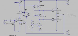
So we were left with a BJT LTP, BJT VAS and balanced FET output... no matter how I tweaked it it was going to look like Rod's design.
Naturally after designing mine, I looked to Rod's site as a reality check. Consequently I borrowed some of his resistor values to help.
So yes, you are right. This is basically a fully current sourced P101!
I wonder how it might sound?
Looks promising though the Idss is still pretty high. Might be workable though.
2SK117 are $0.76 also RS
Don't know which IDSS class they stock
Y: 1.2~3.0 mA, GR: 2.6~6.5 mA, BL: 6~14 mA
There is a spice model about half way down this page
Why did we move away from jfet input devices ? any offset problem is so much easier with jfet or mosfet because they are not affected my impedance so we only have to consider voltage . . . AND jfets have the reputations of sounding better that any other options.
What originally look to me like a nice radical simple design now looks much more like a "vanilla" BJT, cap coupled amp.
DC coupling sounds MUCH better !
I much prefer lineup's final design - to me that is what an amp should be like
What originally look to me like a nice radical simple design now looks much more like a "vanilla" BJT, cap coupled amp.
DC coupling sounds MUCH better !
I much prefer lineup's final design - to me that is what an amp should be like
P.S.
Hi lineup
I am now using multisim V10 and I like it . . . haven't tried V11 yet
but I have no idea what to do when the trials expire
what versions are people using here I wonder - did anyone really pay $2500
thx
mike
Hi lineup
I am now using multisim V10 and I like it . . . haven't tried V11 yet
but I have no idea what to do when the trials expire
what versions are people using here I wonder - did anyone really pay $2500
thx
mike
Mikelm,
I prefer the original one too, especially the one with the single ended input stage.
If you can find me a suitable JFET that is easy to get from a major supplier I'll be happy to build it.
EDIT: My Mistake! I see that Mouser has the 2SK170. Problem solved!
Edit 2: Back to the original design. JFETs ordered!
@tvi:
Thanks for that. I will try to contact RS to find out which model it is....hopefully they will be able to help though I fear they may be ignorant with such matters.
Last edited:
MiiB,
A relevant question as the number of stages should be kept to a minimum. In short, the CFP is much better than the plain source follower.why do you insert an extra driver stage..??
Lumba,
The CFP is NOT superior to the plain source follower in a global feedback topology unless it's used in full blown Class A.
Reason: radical instability at switching point, difficulty with reactive loads, particularly capacitive, and serious tetchiness for bias setting
The CFP is NOT superior to the plain source follower in a global feedback topology unless it's used in full blown Class A.
Reason: radical instability at switching point, difficulty with reactive loads, particularly capacitive, and serious tetchiness for bias setting
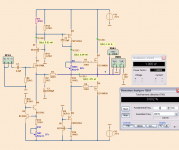
Is this worthwhile
Lineup, all,
Edit: I just noticed that lineup posted a similar LTP config in an earlier post...oops
2SK170s and Laterals are on their way. If we are lucky I might be able to lash up a channel this weekend.
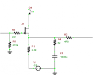
I have been thinking. There are two potential small problems with the single ended input stage:
1) Changing either the load (DC offset) resistor or source resistor will change the current through the JFET meaning the other resistor will need to be changed again - setting the DC offset and current through the input stage will be an iterative process.
2) The JFET might run a little hot.
I thought a way to solve this might be to cascode the input stage with a BC550 BJT (see attached). This means that:
1) The source resistor can be selected out of circuit to give the desired current.
2) Changing the load (DC offset) resistor will not alter the current significantly.
3) Dissipation in JFET is reduced.
4) Because of point 3, more current can be run in input stage.
5) If desired, because of point 4, a larger VAS fet can be used and run at higher current for better performance at high frequencies or paralled ouput stages.
Does this seem like a worthwhile addition?
Cheers,
Greg.
Lineup, all,
Edit: I just noticed that lineup posted a similar LTP config in an earlier post...oops
2SK170s and Laterals are on their way. If we are lucky I might be able to lash up a channel this weekend.
I have been thinking. There are two potential small problems with the single ended input stage:
1) Changing either the load (DC offset) resistor or source resistor will change the current through the JFET meaning the other resistor will need to be changed again - setting the DC offset and current through the input stage will be an iterative process.
2) The JFET might run a little hot.
I thought a way to solve this might be to cascode the input stage with a BC550 BJT (see attached). This means that:
1) The source resistor can be selected out of circuit to give the desired current.
2) Changing the load (DC offset) resistor will not alter the current significantly.
3) Dissipation in JFET is reduced.
4) Because of point 3, more current can be run in input stage.
5) If desired, because of point 4, a larger VAS fet can be used and run at higher current for better performance at high frequencies or paralled ouput stages.
Does this seem like a worthwhile addition?
Cheers,
Greg.
Attachments
Last edited:
Exactly, swordfish
You setup outside of amplifier a JFET circuit to select source resistor Rsource.
Select current. I recommend 4 or 5 mA depending on your supply voltage.
2SK170 is rated 400mW.
So for a supply of 35V we get 5mA x 32V = 160mW
if the voltage across Rdrain is 3V
JFET works better at somewhat higher current. This is why 5 mA.
In your JFET circuit you adjust Rsource until you get wanted current.
After this you pick Rfeedback for example 20xRsource, for gain x20.
Then try to calculate Rdrain. The resistor from VAS MOSFET gate.
If ZVP3310A maybe VGS is 3 Volt. For IRF9610 maybe 3.8V
3V / 5mA = 600 Ohm
Set Rdrain initially to 600 Ohm.
You adjust Rdrain until zero offset at output.
Can of course be done with a potentiometer.
Hi Lineup,
I like this circuit a lot, but I'm concerned that the jfet might need very careful selection, since with a gate biased to ground, a resistor to ground in the source circuit, and another in the drain circuit straddling gate/source on the VAS, there will be fine adjustment required which will drift with temperature and likely create large offset at the output since the fb network will amplify this drift.
The better option might be to restore DC gain to one by placing a 1000uF cap beneath the 27R resistor. This will then permit you to set R1/R12 to a fixed jfet current (which incidentally fixes the loop gain, all other things being equal) and reduce DC gain to unity, giving tight control over offset.
There will now be a return current from the jfet source passing to the series feedback resistor, R5, and this means you will need to bias the gate of the jfet with a positive voltage around 2V. This does involve a bit of circuitry - suggest a LED and diode with a 2K pot, wiper arm to bottom of R6 - but it will give rock solid offset control and there will be no current flow conflicts caused by thermal drift.
Hugh
Hi lineup and AKSA,
Lineup, thank you for all your efforts with the simulator. I managed to get the models to work in LT spice, so now we are both talking on the same wavelength.
I agree with AKSA. The circuit is very touchy as is, even without thermal considerations.
AKSA, I will go home tonight and sim your proposed solution.
Thank you both for bearing with me on this. I have commited to building this amplifier and ordered all the active devices - so your efforts will not simply disappear into a cloud of theory that never gets built.
I like this design because:
1) I can run it in class A / AB with minor modifications.
2) Low parts count.
3) Only 3 stages.
4) Good stability due to SE input.
5) Nice distortion characteristics due to SE input stage.
6) Nice fast "current" feedback.
Sounds like a nice combination to me!
Last edited:
Hi Lineup,
I think you'd get better performance if you stabalized the bias current of the JFET cascode circuit. I think this circuit also adresses Hugh's concern, though I'm not positive.

You could also replace R1 with a current source if you like. Opps, R4 is supposed to be 27 ohms, of course.
I think you'd get better performance if you stabalized the bias current of the JFET cascode circuit. I think this circuit also adresses Hugh's concern, though I'm not positive.
You could also replace R1 with a current source if you like. Opps, R4 is supposed to be 27 ohms, of course.
Attachments
Yes, I think Hugh might be right.
That the weakness of the circuit is offset drift.
It will be intesresting what will be found when swordfishy sets up this amplifier.
Your idea will be one way to address this.
I prefer a current source instead of R1
That the weakness of the circuit is offset drift.
It will be intesresting what will be found when swordfishy sets up this amplifier.
Your idea will be one way to address this.
I prefer a current source instead of R1
AKSA
I do not fancy making a positive 2V at the input terminal.
One of the good things with JFET is the nakedness of the input.
But very probably we need to do something.
We will see that you were right with the real circuit.
I fancy Johnloudb circuit as a remedy.
I do not fancy making a positive 2V at the input terminal.
One of the good things with JFET is the nakedness of the input.
But very probably we need to do something.
We will see that you were right with the real circuit.
I fancy Johnloudb circuit as a remedy.
swordfishy
I am happy but also a bit nervous. 🙂
Now that you will put my circuit to the test.
All the point you have shown why you want to build.
And yes, I loove this circuit.
It is simple, as you say, not many part.
But it shows very good and interesting performance.
🙂
I am happy but also a bit nervous. 🙂
Now that you will put my circuit to the test.
All the point you have shown why you want to build.
And yes, I loove this circuit.
It is simple, as you say, not many part.
But it shows very good and interesting performance.
🙂
I saw Pass ONO used Jfet>Mosfet VAS>Mosfet Output and surely to modify it to best amplifier which contains all lateral VAS (2SK/2SJ) and OUTPUT (2SK/2SJ) 🙂
Last edited:
HI Lineup,
Thanks for the thoughtful post.
When you vary the gate/source resistor on the VAS to achieve zero output offset, you are altering the current through the jfet. As you change the stage current of the input stage, you in fact change the loop gain, which in turn requires a retune of the lag compensation cap between drain and gate of the VAS. This cap is pivotal to stability, and in fact, to sound quality.
The gate of a jfet is a fragile rose, and easily punched through. Any slow moving DC spike at the input could damage it. Solution: Use a zener to ground, and use a blocking cap to block any DC voltage.
It really is no problem to bias the input gate to a small positive voltage. I do it all the time on my Soraya, Maya and NAKSA amps. And it does not change the gm of the input stage!
Hugh
- Status
- Not open for further replies.
- Home
- Amplifiers
- Solid State
- JFET input, MOSFET VAS, LATERAL output = Perfect!!