Hi,
similar to the open source layout from 00940, FauxFrench and I thought about doing a collective project (+ anybody who wants to chime in is of course welcome)
Choice for the power part would be the TDA7293 as it seems to offer good power output, sound quality and is relatively cheap in comparison to the LM3886 for example.
Controlling opamp should just as well be a high-performing but no boutique/expensive opamp. Current state of the art, both from a sound quality and noise/THD point of view seems to be the OPA1656. Alternatives could be a LM4562. (@FF: I have both BTW and could send them to you for prototyping)
There is no schedule to be followed and progress will probably be slow.
It is purely meant for DIY and learning about composite-amplifier-theory and PCB-design and whatever comes to mind along the way.
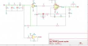
Attached is an premature sketch to get discussion going.
Best regards
Jens
similar to the open source layout from 00940, FauxFrench and I thought about doing a collective project (+ anybody who wants to chime in is of course welcome)
Choice for the power part would be the TDA7293 as it seems to offer good power output, sound quality and is relatively cheap in comparison to the LM3886 for example.
Controlling opamp should just as well be a high-performing but no boutique/expensive opamp. Current state of the art, both from a sound quality and noise/THD point of view seems to be the OPA1656. Alternatives could be a LM4562. (@FF: I have both BTW and could send them to you for prototyping)
There is no schedule to be followed and progress will probably be slow.
It is purely meant for DIY and learning about composite-amplifier-theory and PCB-design and whatever comes to mind along the way.
Attached is an premature sketch to get discussion going.
Best regards
Jens
Attachments
Last edited:
For starters a couple of points that can be decided later on:
- I´d suggest a single TDA7293 for compactness and keeping paths short. (although thanks to the extra pins the chip can be easily paralleled)
- I´m up for an all SMD-parts amp or at least the feedback network/-resistor to keep lead inductances small and maximize stability margins.
But I do know this is not very DIY-friendly.
- Applying a dual opamp as controlling opamp, the second half of the chip could be used as line-out-buffer, headphone output or inverter in order to (opt.) bridge two amplifier-PCBs.
Frankly, the TDA7293 will not make your life easy in a composite. The datasheet is completely silent on important data for a composite amp such as open loop gain graphs.
The distortion goes up quickly with frequency, which doesn't bode well bandwidth wise.
A quick note for the feedback network resistors: as you have to use relatively big resistors to avoid thermal issues, those smd parts would still be quite big.
Btw, there is a composite lm3886 in the open, the ZD50. It's an interesting design to study.
Hi 00940,
everyday listening to your LM3886-PCBs of which I have 4 so thanks again!
Thanks also for the hints. As mentioned this is a pretty premature thought and we don´t know yet where we´re heading.
The datasheet is really scarce so that doesn´t help either but hey it´s for the fun and something different.
There are quite a few LM3886 composites out there. Most not finished though:
Composite amplifier: LM3886 + LME49710
LM3886 composite power amplifier - Share Project - PCBWay
Bridged LM3886 + LME49720 + remote FB
(post 31 in the latter thread)
A few qualitative considerations that may help less experienced DIY’ers to understand what we aim to do. Further, if I am wrong it is possible to correct me before I go too far with useless ideas.
A principle with nested loops is that the simple way to make the combination work is by keeping the bandwidth of an inner element much higher than the bandwidth of an outer loop. The inner element in our case is the power amplifier block. The outer loop is the OP-AMP control loop.
When the inner element has a much higher bandwidth than the outer loop, the inner element has a simple transfer function seen in the operational range of the outer loop. The outer loop will see the inner element as a simple multiplication element between input and output of the inner element. Phase-delay between input and output of the inner element is little significant seen from the outer loop and has less importance for the stability of the outer loop.
Thus, we should use a power amplifier block with a bandwidth as high as possible. The higher the bandwidth of the power amplifier, the higher we can leave the bandwidth of the controlling OP-AMP outer loop. The higher bandwidth of the outer loop, the better suppression of distortion in the power amplifier output. It is mandatory that the inner element is absolutely stable under all normal operational conditions. As the outer loop is much slower than the regulation loop used for the inner element, the outer loop has no chance of compensating for an inner element that misbehaves. Hence, stability of the power amplifier block needs to be ensured before trying to add an outer control-loop.
I tested TDA7293 and some other chip-amps for use in composite amplifiers. The chip-amps were tested the same way but probably not according to a standard. That means that the test results only indicate characteristics of one chip-amp relative to another, subjected to same test.
For TDA7293 I found a -3dB bandwidth of around 600KHz while I found around 400KHz for LM3886. This indicates that TDA7293 should not be inferior to the very often used LM3886.
Chip-amps suited as power stage in a composite amplifier, LM1875/TDA2050 excluded. , posting #33 and other.
Hi Jens,
Sounds exiting. I will add a few postings with considerations before posting a draft of a schematic.
Like you wrote, I hope that we are not in a hurry. I have some other activities to finish at present.
Of audio OP-AMPs I have LM4562, OPA1612, OPA5532 and OPA1622. I can try to get my hands on OPA1656 if needed.
A single TDA7293 is fine with me. It should be quite straight forward to add a second TDA7293 if needed.
My general view on parallel and BTL-coupling: A chip-amp has voltage and current margins that have to be evaluated against to the speaker impedance you intend to use. The limit for the voltage margin is when the output starts voltage clipping. The limit for the current margin is when the output current limiter becomes active.
LM1875 is a chip-amp with very good voltage margin but pretty poor current margin. Therefore a parallel-coupling should be considered.
LM3886 can show some instability at higher supply voltages, but the current margin is fine. Therefore a BTL-coupling should be considered.
TDA7293 has better voltage margin than current margin. Therefore I am more inclined to use a parallel-coupling than a BTL-coupling.
Last edited:
Neat project - I was thinking what would happen if I put an OPA1656 in front of the TDA7293 that I have for the Xmas amp. Have you considered the OPA1642? Much easier to find lately.
I know I need to catch up on nested feedback theory but my current understanding is that the controlling opamp should have a gain-bandwidth product of ~factor 5 higher than the secondary- (here: power-) amp; in order to space their secondary poles far enough apart.A principle with nested loops is that the simple way to make the combination work is by keeping the bandwidth of an inner element much higher than the bandwidth of an outer loop.
You measured the bandwidth in a circuit that is not stable (gain=-5) or am I misinterpreting? What is your reasoning behind this?For TDA7293 I found a -3dB bandwidth of around 600KHz while I found around 400KHz for LM3886. This indicates that TDA7293 should not be inferior to the very often used LM3886.
That was only a suggestion on my behalf based on reviews especially here in the forums and also measurements (I believe Jan Didden measured the OPA1656 and was very impressed:Of audio OP-AMPs I have LM4562, OPA1612, OPA5532 and OPA1622. I can try to get my hands on OPA1656 if needed.
OPA1656: High-Performance CMOS Audio Op Amp, post #371).
An important fact X pointed out is availability. The OPA1612 and 1642 are even available at Reichelt but at more than double the price in comparison with Mouser!
The OPA1611 has been made to work with the LM3886 in this very neat bachelor thesis:
Amplifier Design in a Motional Feedback System | TU Delft Repositories
see pages 13ff (should we just build this and be done? ;-))
@FF: I know you like your veroboards and appreciate the offer to prototype this way. I´d suggest we make a layout and include various compensation schemes (=extra parts in the layout) and just give it a shot (produce a PCB).
But this might be a naive and overly optimistic idea of mine.
And hey, if we fail we can still bypass the controlling opamp and have amplifier boards with TDA7293 ;-)
Last edited:
You measured the bandwidth in a circuit that is not stable (gain=-5) or am I misinterpreting? What is your reasoning behind this?
It was indeed at a gain of 5 I measured the bandwidth. But the TDA7293 was fully stable as the square-wave test proves. In a posting in the next couple of days I will explain why at least I sometimes see and advantage in using the power amplifier in a configuration with a gain less than the minimum gain stated in the datasheet.
OPA1656, OPA1612 or LM4562 is not going to be a big issue. I guess we anyway use an IC socket so members can choose and experiment themselves. Theorectically (datasheet) OPA1612 has slightly lower THD and noise than the OPA1656. OPA1612 has bipolar input while OPA1656 FETs. What sounds best?
A PCB prepared for experiments could be a solution.
Last edited:
OK, understood.
With regards to opamps we can surely try 2-3 different types and see how it sounds. Stability & good function assumed of course.
When I look at the compensations used in that thesis, we are talking about a handful of parts that are (most probably) needed anyway. In place of capacitors (resistors etc.) we could solder sockets like these (cut a single one off) and measure.
https://www.mikrocontroller.net/attachment/197276/MPE_115_1_010.png
This would take the variable PCB a little bit of out of the equation in the search for stability (not that I am an expert in PCB-design but it´s easy enough to better the veroboard I guess).
I´d suppose we start with circuit from the paper above and maybe also that same opamp. Thanks to your measurements the TDA7293 shouldn´t be that far off the LM3886 so that circuit could be a nice fit already.
BTW: If you have a problem with SOIC-packages I can always solder them in before sending the PCBs to you.
With regards to opamps we can surely try 2-3 different types and see how it sounds. Stability & good function assumed of course.
I guess this isn´t much different from the actual final PCB.A PCB prepared for experiments could be a solution.
When I look at the compensations used in that thesis, we are talking about a handful of parts that are (most probably) needed anyway. In place of capacitors (resistors etc.) we could solder sockets like these (cut a single one off) and measure.
https://www.mikrocontroller.net/attachment/197276/MPE_115_1_010.png
This would take the variable PCB a little bit of out of the equation in the search for stability (not that I am an expert in PCB-design but it´s easy enough to better the veroboard I guess).
I´d suppose we start with circuit from the paper above and maybe also that same opamp. Thanks to your measurements the TDA7293 shouldn´t be that far off the LM3886 so that circuit could be a nice fit already.
BTW: If you have a problem with SOIC-packages I can always solder them in before sending the PCBs to you.
Last edited:
I think it is understandable that you want to build a PCB that allows for easy testing, but providing for many options regarding compensation and socketing more components leads to many compromises in layout and adds unwanted parasitics (potentially in locations where you really do not want them). So keep it reasonable I would say.
About the "paper": Let's just say I would rather look elsewhere. Apart from switched OpAmp inputs on one of the most important schematics (Figure 3.12), there are a bunch of other things that leave me scratching my head. I have seen better circuits to use as a starting point on this forum and elsewhere on the web.
About the "paper": Let's just say I would rather look elsewhere. Apart from switched OpAmp inputs on one of the most important schematics (Figure 3.12), there are a bunch of other things that leave me scratching my head. I have seen better circuits to use as a starting point on this forum and elsewhere on the web.
Last edited:
Another thing to maybe include in a first revision.
Look at this circuit with symmetrical clamping diode bridge from jcx:
High loop Gain Composite Op Amp Circuits
Also check out post #27 (same thread) that tries to approximate a composite with TDA7293 in simulation.
Look at this circuit with symmetrical clamping diode bridge from jcx:
High loop Gain Composite Op Amp Circuits
Also check out post #27 (same thread) that tries to approximate a composite with TDA7293 in simulation.
Thanks knoppers.
Yes, sockets are not the optimum and might ultimately not be a good solution.
It works quite well though if everything is properly soldered except this one component you want to fine-tune.
I´m aware of parasitics.
And yes, the schematic has a mistake and by the time of writing the circuit hasn´t been build yet and thus should be taken with a pinch of salt.
SOIC-8 oapmps are pretty easy to desolder with hot air and swap with a new one. They have SOIC-8 to DIP8 adapter boards and I have used those with some success before. I don't think they are bad for a development board.
Jens -- I was going to PM you a bunch of thoughts after you inquired about my (disastrous) simulations years ago, but it's probably best to do here! I'm hoping this project turns out well!
1.) Loop structure I was looking at ended up being a 2nd order integrator around the control opamp, a 2nd order integrator + noise gain on the 7293. This pushes as much of the composite loop gain into the outer loop, where we'll benefit from the greatest distortion reduction. Unfortunately, that makes the compensation complex and component sensitivity. With an open source board, having all those spots available to jumper/populate/test would be fantastic, nonetheless.
2.) My inclination was towards a modern general purpose opamp up front with a good DC offset control, thus eliminating the need for a servo. The ones listed above should be excellent, especially if the target gain is modest. There's also the opa2209, which looked really interesting. Speed shouldn't be too much of an issue as the front end needs to close before the back end.
3.) Has anyone measured loop gain of the 7293? I had meant to do so but woulda-coulda-shoulda. Also, no surprise that G=20 might not be necessary to keep the 7293 stable, especially if it's jumped multiple factories/processes since 1990 or whenever it originally came out. (but no loop gain plots = who really knows?!) But having the loop gain plot will really inform exactly how much internal gain to push into the outer loop.
4.) JCX's clamp circuit is pretty brilliant, if needing to be empirically tuned!
5.) I also thought about making an instrument amp up front (with a g < 1) and then using the composite as the summing amp (where the g < 1 front end gives us more room to raise gain in the composite making compensation much easier, if a little less ideal noise-wise).
Many thanks for putting your thoughts down here, Daniel!
They might help at one point and give us a direction.
Looks like we´ll have to rely on measurements quite a bit (there are spice models though for all the typical "OPAs" we talk about like 1611/1612)
Have to talk to FF about what and how to measure.
Would love to measure the open loop gain myself.
We have half a dozen network analyzer at work but each costing between a Volkswagen and a Lamborghini. If anybody sees me connecting a 3€ chipamp with +-40V supply to those they probably shoot me to the moon!
At the moment I only do have access to an oscilloscope.
Eventually I can borrow a signal generator (for step responses).
Just thinking out loud:
If we would apply the minimum gain from the datasheet to the TDA7293 (26dB) that wouldn´t leave much gain for the controlling opamp. (assuming we don´t need/want >30dB gain; I personally would be fine with 20dB or even less)
FF has shown function of the chip with a gain of 5 and but I think that has to be tested further and I´m still sceptic this could work out in a stable way unless we test this with signals of all frequencies, levels and shapes.
As it seems the TDA7293 can be used as power buffer which could eventually be a solution that would make the composite arrangement much simpler.
A 100W or so buffer for 3€? That would be amazing!
Unfortunately I can´t find much info about that other than this little thread here from 10+ years ago:
TDA7293 as output stage
So it would be one of the things that could be tested on the way and could make for a simple and stable solution.
Drawback obviously would be, the need for a driving stage that makes use of the TDA7293 output capabilities.
A simple solution would be a OPA604 for example that could at least provide a voltage swing of about roughly +-20V (assuming +-24V supply voltage) and thus about 25W into 8Ohms.
Absolutely fine with me as long as it works and sounds as good as we´d like.
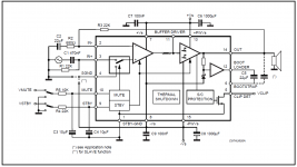
Another drawback is (as it seems from the block diagram in the datasheet) we´d skip some of the protection-/mute-circuitry. It looks as the thermal protection is also located before the buffer. That would leave just the short-circuit-protection active. But these are just guesses!
If we would apply the minimum gain from the datasheet to the TDA7293 (26dB) that wouldn´t leave much gain for the controlling opamp. (assuming we don´t need/want >30dB gain; I personally would be fine with 20dB or even less)
FF has shown function of the chip with a gain of 5 and but I think that has to be tested further and I´m still sceptic this could work out in a stable way unless we test this with signals of all frequencies, levels and shapes.
As it seems the TDA7293 can be used as power buffer which could eventually be a solution that would make the composite arrangement much simpler.
A 100W or so buffer for 3€? That would be amazing!
Unfortunately I can´t find much info about that other than this little thread here from 10+ years ago:
TDA7293 as output stage
So it would be one of the things that could be tested on the way and could make for a simple and stable solution.
Drawback obviously would be, the need for a driving stage that makes use of the TDA7293 output capabilities.
A simple solution would be a OPA604 for example that could at least provide a voltage swing of about roughly +-20V (assuming +-24V supply voltage) and thus about 25W into 8Ohms.
Absolutely fine with me as long as it works and sounds as good as we´d like.
Another drawback is (as it seems from the block diagram in the datasheet) we´d skip some of the protection-/mute-circuitry. It looks as the thermal protection is also located before the buffer. That would leave just the short-circuit-protection active. But these are just guesses!
Attachments
I was wrong I guess. Here is some distortion measurements of the TDA7293:Unfortunately I can´t find much info about
https://www.diyaudio.com/forums/chip-amps/197398-tda7293-single-bridge-parallel.html#post2729693
In post #12 it starts to get interesting. TDA7293 applied as buffer but with pretty high distortion. Pin 11 seems to have a low input impedance so the setup might have been sub-optimum and the shown THD misleading.
Post #86 and following things start to get interesting again. A LME49811 in composite with the TDA7293 buffer working and with pretty good distortion levels.
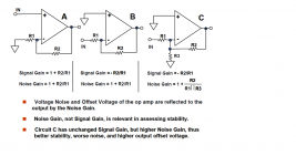
Did you ever try to use a signal gain of 1 (inverting) but introducing noise gain of about 26dB (->minimum gain from datasheet); circuit C from picture. That should definitely be stable and make the composite rather easy to handle.In a posting in the next couple of days I will explain why at least I sometimes see and advantage in using the power amplifier in a configuration with a gain less than the minimum gain stated in the datasheet.
That would of course mean that the noise and thus S/N-ratio would get about 26dB worse.
Signal gain of 4 (12dB) and noise gain at 26dB would still be S/N-loss of 14dB.
That said, in the composite the overall noise could still be better than a single TDA7293 (assuming a very low-noise controlling opamp).
Picture taken from MT-033 tutorial (Analog Devices):
https://www.google.com/url?sa=t&rct=j&q=&esrc=s&source=web&cd=&cad=rja&uact=8&ved=2ahUKEwiGhbjLwajvAhWFr6QKHR5QAxsQFjAAegQIBBAD&url=https%3A%2F%2Fwww.analog.com%2Fmedia%2Fen%2Ftraining-seminars%2Ftutorials%2FMT-033.pdf&usg=AOvVaw2tNPmBlfid2O50Ov_Ok6th
Attachments
Last edited:
Just realize that this is plain wrong.🙄That would of course mean that the noise and thus S/N-ratio would get about 26dB worse.
Signal gain of 4 (12dB) and noise gain at 26dB would still be S/N-loss of 14dB.
That said, in the composite the overall noise could still be better than a single TDA7293 (assuming a very low-noise controlling opamp).
In order to calculate the actual worsening of the S/N one would have to know the actual noise that is being amplified but you get the point. Noise in that configuration would be amplified with a factor of 20 and the signal only between 2-5x, if applying reasonable gain in that inner (power) loop.
- Home
- Amplifiers
- Chip Amps
- Open source layout for a TDA7293 composite amp