As it seems the TDA7293 can be used as power buffer which could eventually be a solution that would make the composite arrangement much simpler.
A 100W or so buffer for 3€? That would be amazing!
OPA547 can drive +/-30v and might be useful.
https://www.ti.com/lit/ds/sbos056f/sbos056f.pdf?ts=1615444499344
Hi Jens,
Nice to see so much energy and enthusiasm.
I only tried the TDA7293 down to a gain of -3 and made most tests at -5 simply because you cannot find an audio OP-AMP that can drive a TDA7293 to near clipping with good supply voltage if the TDA7293 operates with unity gain. You will soon conclude that a gain of 5 (or 5) is far more useful. You can do that buffer trick with less powerful chip-amps.
We used the LM1875 with a gain of -3.5 and arrived at a power-buffered LM4562 that could pull an 8 Ohm speaker to almost 100KHz, if I remember right. DC to almost 100KHz with low THD. The construction was very modest in number of parts but I used fake LM1875 and that was fatal in the end.
My impression is that when you force the closed-loop gain of a TDA7293 down below its natural lower stability limit, you increase the THD somewhat (some say mainly for common-mode signals) but you can increase the OP-AMP noise gain to compensate.
I have seen TDA7293 behave like a -5x power block with an impeccable stability and no visible distortion on my scope for the audio range. It worked with an LM1875 at -3.5x so I am convinced that the same will work with the TDA7293 at -5x. Apart from that the TDA7293 will give more power at the output.
Posting #46 at this thread: Chip-amps suited as power stage in a composite amplifier, LM1875/TDA2050 excluded.
More to follow…………..
Did you ever try to use a signal gain of 1 (inverting) but introducing noise gain of about 26dB (->minimum gain from datasheet); circuit C from picture. That should definitely be stable and make the composite rather easy to handle.
Jens,
Make sure you're thinking about the problem correctly. (And make sure to read Jerald Graeme and Jim Williams applications notes) The outer loop will determine the overall closed loop gain whereas the amplifiers will respectively contribute to the loop gain. So we want as much loop gain being pushed into the outer loop, where it has the greatest distortion reduction capability, but need to temper this with stability, which is where compensation and gain shaping come into play. Burning away 26 dB of gain broadband and reducing the outer loop gain contribution of the 7293 to 1 doesn't benefit you noise/gain wise, and means that the input opamp has to swing all the way to the rails of the 7293 (less the internal drop of ~4V), whereas using the 7293 as an integrator with a safe phase margin near unity gain means 20-80 dB of gain is pushed into the outer loop through the audio band.
Didn't read it too too carefully, but seems to cover the space well: https://www.analog.com/media/en/ana...gh-output-drive-capability-with-precision.pdf
OPA547 can drive +/-30v and might be useful.
https://www.ti.com/lit/ds/sbos056f/sbos056f.pdf?ts=1615444499344
I tested the OPA549 for this use and that was a disappointment:
Posting #125: Chip-amps suited as power stage in a composite amplifier, LM1875/TDA2050 excluded.
It showed cross-over distortion, was pretty slow (slew-rate), had interference from a thermal limiter and was not worth the price I paid. I can compensate cheaper chip-amps to perform better than that.
But, your idea is logical.
My view on the power amplifier block in a composite amplifier construction is the following:
The power amplifier block should be designed to have ensured stability under all reasonable conditions of operation, have a bandwidth as large as possible and the amplifier block should have a closed-loop gain that is best for the composite amplifier construction as a whole.
Stability of a chip-amp can be ensured either by staying within the closed-loop gain specified in the datasheet (for TDA7293: 26dB minimum, 30dB recommended) or by modifying the loop-gain if a closed-loop gain outside of the datasheet specification is clearly preferable for other reasons.
An issue I find important for the composite amplifier construction is the amplitude operational conditions for the controlling OP-AMP and the power amplifier block. A reason is that any audio OP-AMP has a distortion curve (THD+N as function of output amplitude) that decreases steadily from very little amplitude and until an amplitude where the distortion suddenly raises very fast.
For LM4562, such curves are shown in the datasheet figures 3-14. With a supply voltage of +/-15V, an LM4562 has least THD+N at 4-5V (effective) amplitude (2K loading).
For OPA1612, such a curve is shown in the datasheet figure 11. With a supply voltage of +/-15V, an OPA1612 has least THD+N at 9V (effective) amplitude.
For OPA1656, such a curve is shown in the datasheet figure 11. With a supply voltage of +/-15V, an OPA1656 has least THD+N at 7-9V (effective) amplitude.
When the OP-AMP THD+N starts raising fast due to the output amplitude, the power amplifier block should start clipping. Like that, the OP-AMP is used with least THD+N. When the power amplifier block starts clipping it is not important that also the THD+N of the OP-AMP is raising fast.
Assuming that we intend to use the TDA7293 to a clipping level of 40Vp (supply voltage of +/-43Vdc), we can calculate the gain needed in the power amplifier block (closed-loop gain).
4.5Veff corresponds to 6.4Vp; 9Veff corresponds to 12.7Vp; 8Veff corresponds to 11.3Vp.
For LM4562: 40Vp / 6.4Vp = 6.3 x gain.
For OPA1612: 40Vp / 12.7Vp = 3.2 x gain.
For OPA1656: 40Vp / 11.3Vp = 3.5 x gain.
For natural stability of the TDA7293, a minimum gain of 20 is specified but a gain of 32 is recommended. That would mean that the OP-AMP would operate at amplitudes much below where it has its best performance. We would operate left of the minimum THD+N shown in the curves.
My impression on noise contribution is that a TDA7293 is significantly more noisy than an audio OP-AMP and that the noise from the TDA7293 increases with its closed-loop gain. If I am right, keeping the power amplifier block gain down introduces less noise in the outer loop and increasing the OP-AMP gain instead leaves less noise in the system. We could in principle obtain a resulting gain of 5 by first scaling the signal down with a voltage divider and then following let the TDA7293 boost the signal with 30dB. But, with my understanding it would be a noisy solution.
My previous tests of the TDA7293 showed that it could be “tamed” at gains much below the minimum gain specified in the datasheet, with a surprising stability and seemingly with moderate distortion.
To be continued...........
Last edited:
Questions about the power amplifier block are inverting or non-inverting configuration? And, DC or AC coupling?
For the LM1875 we chose inverting configuration. The OP-AMP doesn’t care and the inputs just have to be used accordingly.
Empirically we found that the LM1875 was easy to stabilize at very low gains when used in an inverting configuration. I can imagine some reasons: The gain of an inverting configuration is the feedback resistor divided by the input resistor. The gain of the non-inverting configuration is the same plus one (+1). Though we all like to get something for free, it can be inconvenient when you aim for a lower gain than natural stability recommends. The teaching from a minimum closed-loop gain to ensure stability means that the harder we feed back, the further we risk instability. If we would like the power amplifier block to have a gain of for instance 5, we can either use an inverting configuration where the feedback results in a gain of 5 or we can use a non-inverting configuration where the feedback results in a gain of 4 plus the 1 that comes “for free”. Thus, using the non-inverting configuration we use harder feedback than with the inverting configuration for the same overall gain. Hence, the chip-amp loop is a little less far away from natural stability with the inverting configuration. I have been told that reducing amplifier gain with a resistor between the two input pins increase distortion but in particular for common mode signals. Assuming that is correct, the inverting configuration is based on differential input signals only while the non-inverting configuration partly uses the input signal common-mode wise. Thus, two reasons indicating that the inverting configuration could be preferable.
In the thread which I have been referring to a couple of times, I tested various chip-amps only in inverting configuration with the purpose to show that there was a solution and more-or-less how that solution looked. It was no proof that the inverting configuration is superior to the non-inverting configuration. But, use of the non-inverting configuration requires that someone repeats my inverting tests for the corresponding non-inverting configuration and compares the results.
The controlling OP-AMP needs a feedback-response to all frequencies it tries to regulate, hence, to all signals it receives on its signal input. If we use a non-inverting power amplifier block, its resistor to the inverting input may be connected in series with a capacitor such that the resulting gain at very low frequencies becomes 1. This non-inverting coupling is useful for normal chip-amp circuits where we want to reduce the DC-offset at the output. In a composite amplifier with an outer controlling loop, the outer loop compensates for DC-offset in the power amplifier block. With this outer control loop, the DC-offset at the output becomes the DC-offset at the OP-AMP input times the closed-loop gain of that outer loop. An LM4562 has a typical input offset of 0.1mV. With a closed-loop gain of 10 (20dB), the DC-offset at the output will be 1mV. With a gain of 20 (26dB) the offset becomes 2mV. OPA1612 has an input offset similar to the LM4562 and the results become the same. OPA1656 has five times the offset of an OPA1612 such that the results at the output become 5mV and 10mV.
I find that even 10mV is nothing to worry about and a DC-servo or even manual regulation is unnecessary. Accordingly, I see no reason why the power amplifier block cannot be DC-coupled to the outer loop such that less components are use and the transfer function becomes the simplest. Very low frequency cut-off (some 5Hz) is then arranged at the input of the outer loop.
Thanks everybody for some good food for thought.
And excuse the sometimes half-axxed musings but I think it´s important to note what we know and what we don´t.
I´m with you FF, the TDA7293 in an inverting-configuration with a gain of 5.
In any case I´d like to include R3 from the circuit I posted above (post #19):
1. this way one can ensure stability of the inner loop under most circumstances
2. in case of oscillations one can better isolate if its triggered by the inner or outer loop. When not needed just replace with a wire, or 0R SMD-resistor.
I understand your reasoning for a gain of 6.3x for the LM4562 but if we end up with a gain of 30dB (5x6.3), that would mean more attenuation in front of the composite and thus more noise at typical listening levels.
I do believe the "first watt" is most important and don´t care so much about the performance of an amp where my ears already bleed ;-)
That said, this is not something that we necessarily have to define before (opamp & gain of control loop).
As I see it, the "only" things left open in the schematic is compensation(s), parts we gonna use(decoupling, SMD/through-hole, voltage regs. for the opamp, max. supply +-43V?) and which parts we have to expect to change in the process of evaluation (-> these go in the top layer and preferably non-SMD).
And what do we have in our drawers to keep cost down.
Last edited:
Of course this point will be contradicting in places:which parts we have to expect to change in the process (-> these go in the top layer and preferably non-SMD)
The feedback paths should be kept as short as possible which could mean putting parts under the TDA7293 or using SMD (which also isn´t too easy to change) but as you have more practical experience in composites and their sensitivity to layout i´ll stick with your opinion about that.
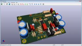
This is just a draft (parts placing) to whet the appetite and to get a feel for the size of the board and critical areas. You can see the feedback resistors on the bottom layer next to the TDA7293. (this PCB is 80x55mm)
(If you´re ready we will do the layout together, be it next week or in 2 months.)
Attachments
Hi Jens,
Sorry for the "holes" in my response.
We seem to agree a lot. R3 is just what I want as well. I will even suggest a resistor (R4) between the non-inverting input and ground such that R3 is connected directly between the two input pins and R4 goes to ground. This was how I tested various chip-amps in the other thread and an R4 seems to leave the possibility for further gain reduction.
I fully understand that a SOIC-8 OP-AMP can be replaced but for those of us who like to experiment, I prefer a DIL-8 socket and use of SOIC->DIL-8 converter boards. This is how I use my OPA1612.
I will also suggest an OP-AMP output clamp. It is basically two zener-diodes connected in series back-to-back and a small value resistor. This clamp catches the OP-AMP output when the power amplifier block starts clipping and the OP-AMP looses feedback (due to the clipping saturation).
Last edited:
I have been toying with the TDA 7293 for some time and I find it very interesting for a number of reasons.
The LM3886 which is extremely popular has a few limitations the main one being the maximum power it can produce. Of course it can be paralleled but this is where it gets tricky , requires the use of very low tolerance components etc.etc. It is a childs play to use two or more TDA 7293 in parallel since that use has even been designed into them , and is is a lot cheaper than the LM3886 so no problem there. Provided one gets the real thing and not the " Chineasy fakes from XYZ " . Mouser is a good reliable place for that.
On the other hand they need very good cooling if you want to get more than 15 to 20 W out of them with the added inconvenience of the casing being connected to the negative rail so they need to be insulated via mica or be on an isolated heatsink or fans. The Achilles heel of these chips is their max dissipation. only 50 W at 70 degrees
This is a nice DIY-challenge though which I have tackled by interposing a 4 mm copper-plate so that the TDA´s are bolted directly to that using Arctic Silver and the copper-plate to the heatsink using normal thermal compound with Kapton-tape to bolt it electrically insulated to the aluminum-heatsink. It reduces the chips temperature by up 20 degrees
at high power compared to chip on Aluminum via mica. Keeps the heatsinks from becoming monsters.
What I like about them is the fact that one can build a 12" or 15" Sub-woofer amplifier in a 2x parallel-BTL configuration keeping the rail voltages relatively low say 2 x 40V torturing said woofer while at the same time using two single chips one for mid-bass and one for the tweeter . It has a lot more potential to develop different solutions than does the LM3886.
so " Taming the TDA7296 " and " TDA7293 done right "could be an extremely interesting project
Last edited:
MalleMike, how is Mallorca?
This is pretty much off-topic but I give you my view anyway.
Both chips are pretty similar and of course they have limitations but in comparison they are pretty rugged devices.
Look at an amp with 2SC5200/2SA1943. Much easier and quicker to destroy due to SOA violations. (40V/4A or so IIRC)
If you want it to do more than the LM3886 you will have to parallel devices and then it´s not a fair comparison anymore.
Pd of 40W is not that limiting either. Design your circuit properly and you´re fine. Bridge, parallel. Look in the Passlabs forums. Lots of designs with Pd=40W/device and these run that dissipation permanently.
To say this is an Achilles heel is ignorance of the facts.
Your method of mounting the TDA sounds good to me. We do similar things at work. In the DIY world you can take a design to such extremes, although it would be much more sensible to bridge/parallel to keep Pd down.
Yes, this is an interesting project but we will work mostly empirically and thus I wouldn´t compare this project to anything TomChr does.
That said I hope we will arrive at a point where we measure THD, freq./phase response later.

Interesting. What is the ration between current and voltage feedback?
Slow on math...
Does anyone have spicemodel for TDA7293/TDA7294 ?
Slow on math...
Does anyone have spicemodel for TDA7293/TDA7294 ?
Hey people,
is this project still alive?
I'd really like to build a TDA7293 composite amp 😉. I am just ordering PCB's and put 5 TDA7293 Christmas Amps in the shopping cart. Maybe next time there could be a TDA7293 composite? I'd love to help, but I'm just a mechanic ... .
is this project still alive?
I'd really like to build a TDA7293 composite amp 😉. I am just ordering PCB's and put 5 TDA7293 Christmas Amps in the shopping cart. Maybe next time there could be a TDA7293 composite? I'd love to help, but I'm just a mechanic ... .
Thanks for the reminder😉
It is still alive but you know, we all got things to do;
like moving flats and changing jobs.
I´m pretty sure there is gonna be progress soon.
We have created a revision of a PCB which we hopefully will get to work.
I´m gonna start populating mine in about two weeks and start to measure.
I will get back as soon as we have something to discuss, present and after I had a word with FauxFrench (who also has some PCBs).
But don´t expect anything too soon.
This might not work out as the next TDA7293 xmas amp😉
@joensd
Hi
If you chose a op amp for EC , chose the one with character of dominant H2 distortion.
TDA7293 have a natural H2 dominant character which is unusual for a Chip amp and found mainly in fine tuned Dis-create Class AB amplifier.
I will recommend adding a DC Servo to eliminate NFB cap , It will improve transient response and slew rate. All 7293 i measured have slew between 11v/us to 19v/us ( Bit erratic)
I am wishing your project to come alive
Thanks Dibya,
lovely to get advice from somebody knowing the TDA7293 as well as you!
We shall keep that in mind when there will be another revision of the PCB.
As I said, we hope to have some progress soon.
The fact that I ordered a preliminary version of the PCB (without initially posting it here for discussion) was due to the fact that I ordered other PCBs and had a timeslot for designing it.
I have a suggestion , maybe its crazy , maybe its not, The best composite amp I´ve seen so far is the modulus from Tom , at Neurochrome.
Using that circuit diagram as an informative base it should be possible to develop a modified version for one or more than one TDA 7293 and a more powerful one , especially if one designs for 50 volt rails from the very start.
Of course its a very big modification , the result is sure to be a completely different circuit . Maybe even Tom himself could do it as he is probably the most competent and knowledgeable member of this here forum concerning composite amps , if he were to find it in himself to do this.
Please do not take this as an intent to copy his merits or circuit but the study of how he has done it should provide a good insight into the possible ways to solve it and to avoid some of the inevitable errors on the way. ,so using his circuit as information and learning from it should at least serve to point the way.
I am not enough of an engineer to tackle this myself so all I can do and contribute is to try to find a good and correct way towards getting a truly well done chipamp based on the TDA and hope to find the necesary others here to get there with a common effort .
Last edited:
- Home
- Amplifiers
- Chip Amps
- Open source layout for a TDA7293 composite amp