I am now onto the FE cards and my jfets are not the ones in the guide so to be on the safe side I would like to confirm the proper N and P channels of these ones. Am I wrong assuming that these are ok for this build,I am pretty sure they are just trying to not be in the explosive club!🙂 Picture attacked ,thanks.
Attachments

Yes, there are just Linear Systems (LS) and not the original Toshibas (2SK). They should be about identical in performance.....
View attachment 944765
In case anyone is interested, I found some quasi inexpensive aluminum feet that actually grip instead of the felt bottomed stock ones. It visually looks similar and is within 2mm O.D. Of the stock feet.
https://www.amazon.com/dp/B07QL285T...abc_8CXGEJFZQT3EF4XF2TMC?_encoding=UTF8&psc=1
Oooh, I always wanted sand blasting feet. Totally jumping on the bandwagon... Ordered!

These are more than OK, I think! These are the very coveted jfets that will populate most of the FirstWatt clones! I think these are actually "better" than the ones described in the BOM.I am now onto the FE cards and my jfets are not the ones in the guide so to be on the safe side I would like to confirm the proper N and P channels of these ones. Am I wrong assuming that these are ok for this build,I am pretty sure they are just trying to not be in the explosive club!🙂 Picture attacked ,thanks.
To get these is a real treat, IMO!
Rafa.
The problem with very efficient speakers like +105dB is that there might always be a "hiss-sound" as "background". It requires that there is just enough gain and ACP+ could be a perfect amp for the Klipsch as the only amp?
The input impedance of the output stage is over 100K, and relative
capacitance is low, so the only preamp issues are gain and voltage swing.
13 volt input will take it to clipping but 4 volts or so will make a pair of
La Scalas get up and dance.
Well that's good to hear I am long overdue for a treat. Here they are soldered in then tucked in a sandwich with a bit of silver paste and my last piece of heat shrink.
Attachments
I dunno...it really pushes the limit scale-wise. It's larger than the logo. But if you like it, what does my opinion matter?! 🙂
My PS and FE boards are done. The OS boards will probably be completed tomorrow. I'm waiting on missing fasteners and hope that number 12 will be up and running sometime next week. Can't wait!
Muchos albondigas to NP, the diyAudio team, HiFi2000 and pfarrell!
Regards.
Muchos albondigas to NP, the diyAudio team, HiFi2000 and pfarrell!
Regards.
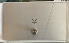
Cutting the necessary 25mm hole without damaging the printing or surface finish will be a bit of a trick, but I think can be done with some care.
I'm planning to protect the surface with some temporary shelf paper during machining. Alas, I don't have a Bridgeport mill at my disposal, so a drill press & hole saw will probably have to do.
Any other suggestions on how best to cut the hole cleanly in a panel this thick without resorting to a milling machine?
I dunno...it really pushes the limit scale-wise. It's larger than the logo. But if you like it, what does my opinion matter?! 🙂
Yes, it is pushing the size a little bit. I could step down to a smaller diameter - the trick will be finding one with threads deep enough to reach all the way through the 10mm panel thickness.
... and part of my reason for posting was specifically to solicit some feedback. So thanks - I do appreciate your opinion. Don't want to do something irreversible that I might regret later.
I'll have to stare at it a while longer and see if I really like it or not.
Last edited:
The depth is concerning. I did a similar process with a drill press, but on a 3mm aluminum.
The problem is that the heat starts changing the anodizing color and shine... it makes it kind of "rainbowy".
My suggestion would be to grow incrementally in sizes: start with simple drills (not the ones with "wings") of smaller diameters and step up. This will produce the least friction, minimizing the chances of overheating the metal.
Still, 15mm is a really different ball game. I would be a bit scared. 🙁
Hope it turns out nice... it certainly looks good, and is a really useful addition.
Rafa.
edit: Also, you have to really secure the piece so that it doesn't start turning along with the drill, or it will really kill it. I know it's "obvious", but with such depth, the friction can be enormous!, and hard to secure.
Last edited:

Is there a general consensus that it is beneficial to thermally couple both jfets? (even if done front to back?).Well that's good to hear I am long overdue for a treat. Here they are soldered in then tucked in a sandwich with a bit of silver paste and my last piece of heat shrink.
I guess I could put an aluminum sheet between them and wrap them with a plastic fastener. Do you think that would be useful at all? Or detrimental if it is not done 'properly'?
Thanks.
Rafa.
As of one hour ago #105 is alive.
Mid point on the pots gave me 19.3 and 18.7V on start up.
Thanks for Mr Pass for putting this together!
Some notes to share:
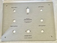
The top and bottom plates are directional. If you do not know this you may put the PS board on the wrong end and not realise this until you put the end panels on. The longer end goes to the rear.
Idling for one hour puts the heat sinks at 45 with a IR thermometer.
Thump on power off and power on.
Mid point on the pots gave me 19.3 and 18.7V on start up.
Thanks for Mr Pass for putting this together!
Some notes to share:
The top and bottom plates are directional. If you do not know this you may put the PS board on the wrong end and not realise this until you put the end panels on. The longer end goes to the rear.
Idling for one hour puts the heat sinks at 45 with a IR thermometer.
Thump on power off and power on.
Last edited:
Any other suggestions on how best to cut the hole cleanly in a panel this thick without resorting to a milling machine?[/QUOTE]
If you look on the back side of the front panel, mine had three holes in a line, the center hole for the LED.
You hit one of those with a hole saw and you may end up with a larger than you wanted oval hole.
With out a milling machine, a 1" hole is.......
If you look on the back side of the front panel, mine had three holes in a line, the center hole for the LED.
You hit one of those with a hole saw and you may end up with a larger than you wanted oval hole.
With out a milling machine, a 1" hole is.......
Is there a general consensus that it is beneficial to thermally couple both jfets? (even if done front to back?).
I guess I could put an aluminum sheet between them and wrap them with a plastic fastener. Do you think that would be useful at all? Or detrimental if it is not done 'properly'?
Thanks.
Rafa.
No real point in this design, because the output of the front-end buffer is cap coupled to the transformer. If it were DC coupled at the output, then the thermal drift due to temperature difference between the two FETs might matter, and benefit from a tight thermal coupling.
- Home
- Amplifiers
- Pass Labs
- DIY Sony VFET Builders thread