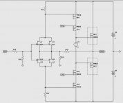
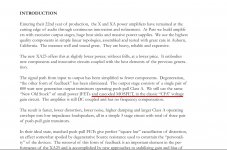
Well, the online XA25 manual reads:
- Degeneration, “the other form of feedback” has been eliminated.
- The output stage consists of a single pair of 800 watt new generation output transistors operating push-pull Class A.
- We still use the same “New Old Stock” of small power JFETs and cascoded MOSFET, in the classic “CFA” voltage
gain circuit.
- The amplifier is still DC coupled and has no frequency compensation.
...
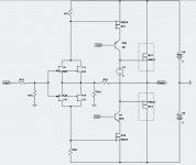
This changes the schematics above to include two cascode transistors:

Last edited:
contemplations are mostly in F4 beast builders thread
there you'll find links to few tests with pictures , so you can see that none of your schematics is precise guess
it's more like BA3 FE (with input JFets cascoded , that more likely than mosfet drivers cascoded ) with few heavy twists following in OS itself
there you'll find links to few tests with pictures , so you can see that none of your schematics is precise guess
it's more like BA3 FE (with input JFets cascoded , that more likely than mosfet drivers cascoded ) with few heavy twists following in OS itself
Last edited:
contemplations are mostly in F4 beast builders thread
there you'll find links to few tests with pictures , so you can see that none of your schematics is precise guess
it's more like BA3 FE (with input JFets cascoded , that more likely than mosfet drivers cascoded ) with few heavy twists following in OS itself
Thanx for the info.
However, there is no mention of cascoded input JFETs in the manual, but the online manual clearly states cascoded Mosfets:
" We still use the same “New Old Stock” of small power JFETs and cascoded MOSFET, in the classic “CFA” voltage gain circuit."
Cheers...
Attachments
Last edited:
I know that
but , if you take a look at pictures , you'll see just one pair of obvious candidates for cascode duty ..... and if they're taken by mosfets , that leaves tiny input JFets exposed to highish rails
so , it's more likely other way - input JFets are cascoded , so being umbrella-ed from excessive voltage , while mosfet drivers are
anyway , these contemplations are not near most important thing in XA25 - which is biasing mechanismus of hockey pucks - where exactly sensing is , and where exactly biasing is situated (how far to input side)
FE is sort of trivial to that ......... just follow all Papa's breadcrumbs we already have scattered all around

if you rephrase it ( as "power" being culprit term there ) as :
" We still use the same “New Old Stock” of cascoded JFETs and small power MOSFETs, in the classic “CFA” voltage gain circuit."
that could explain pictures ....... (especially if we know that small power JFet's are pretty rare breed)
besides , what's typo here and there , between friends ?

I know that
but , if you take a look at pictures , you'll see just one pair of obvious candidates for cascode duty ..... and if they're taken by mosfets , that leaves tiny input JFets exposed to highish rails
The PSU rail voltages for a 25W amplfiier is around 20 Volts.
That is not excessive for the input JFets.
However, you might be right: that is the input JFets might very well be cascoded.
But remember, there is no mention of it in the XA25 manual, and I dont see why Mr Pass would not want to mention that.
so , it's more likely other way - input JFets are cascoded , so being umbrella-ed from excessive voltage , while mosfet drivers are
anyway , these contemplations are not near most important thing in XA25 - which is biasing mechanismus of hockey pucks - where exactly sensing is , and where exactly biasing is situated (how far to input side)
FE is sort of trivial to that ......... just follow all Papa's breadcrumbs we already have scattered all around
From an electrical point of view, it is more beneficial to cascode the second stage Mosfets - the ones you call drivers, sine they need to run at quite high bias current levels.
Last edited:
well , your thinking have some logic
feel free to try your own ideas in vivo ,same as any other Greedy Boy around
I have my own interest in possible deciphering of Papa's circuit - to learn something new , not to have XA25 knock-out
edit: sole small power JFet I'm aware of is LU1014 , used in F3 circuit
feel free to try your own ideas in vivo ,same as any other Greedy Boy around
I have my own interest in possible deciphering of Papa's circuit - to learn something new , not to have XA25 knock-out
edit: sole small power JFet I'm aware of is LU1014 , used in F3 circuit
Last edited:
Zen Mod, are you referring to the comment by Ihlquam here?
http://www.diyaudio.com/forums/pass-labs/300233-f4-beast-builders-52.html#post4962020
According to him , the manual is written wrong.
That is the input JFets are cascoded and "driver" Fets are connected as complementary CS stages with no cascode Q's.
http://www.diyaudio.com/forums/pass-labs/300233-f4-beast-builders-52.html#post4962020
According to him , the manual is written wrong.
That is the input JFets are cascoded and "driver" Fets are connected as complementary CS stages with no cascode Q's.
----------------------------------------...I have my own interest in possible deciphering of Papa's circuit - to learn something new , not to have XA25 knock-out
The name of this thread is Pass XA25, so I think discussing the possible implementations
of the XA25 circuit is VERY relevant, not other things like the BA3 or other designs.
It appears that there has been a mistake in the literature (owners manual) of XA25.
However the manual clearly states the cascoding of the second stage Mosfets and not the input JFets.
As I stated earlier, cascoding the input JFets makes very little sense, specially in reference to the
XA25 literature, and the fact that the PSU voltages applied to the circuit are quite low.
Cascoding the second stage Mosfets are very beneficial in such a simple design, with only one drawback: limiting the output voltage swing.
Parallelling the input JFets has many benefits in this particular design, and it is likely that it has been implemented in the XA25.
Last edited:
logic is perfect ........ if you believe that Pa is feeding pucks with so low voltage (think of massive inter-electrode capacitances)
I know that I wouldn't ...... but that's just me
-----------------------------------------------
I'm sorry, but your comments are very unclear.
Looking at the distortion measurements presented by Pass Labs, XA25 exhibits very low distortion
over a wide bandwidth.
This would be pretty difficult to obtain with an equivalent circuit-design to the BA3 front end.
----------------------------------------------I'm from Serbia , you're from Sweden ..... both writing in English
what's there to be clear ?

No, I do not mean your language. We all have problems with the english language ;-)
I do not know what "Pa" or "pucks" is. So THAT makes the text difficult for ME (not for other people) to understand.
Lets get back to the subject at hand:
I would appreciate any suggestions on possible XA25 circuit implementation from other members here.
My best guess is that the input is possibly a double complementary JFets, possibly connected in parallell, with
cascoded 2nd stage complementary CS stage running possibly on a second, higher PSU voltage.
The Cascode transistors might even be bipolar transistors, what are other memeber's thoughts?

BTW, are there any good pics of the interanl of the XA25? I couldnt find any :-(
Last edited:
you know ..... you wrote , I replied what I think
however , I'm not arguing and preventing you to beat your own bush
what you obviously don't know is that we usually have around collective bush beating, so when I pointed you to right thread , after reading this one in entirety , that wasn't not for nothing .
Pa is Papa is Nelson
pucks are hockey pucks are IXYS outputs in very XA25
BA3 FE is very well known swiss knife type front end circuit made by , surprise, Papa
bigger plastic devices on XA25 FE pics (which you obviously didn't bothered to find in pointed thread) are strikingly similar to fave Papa's bipolars deliberately used as cascode devices in PL products
on same pics you'll see just pair of T092 devices per channel ; PL is not having habit of piggy-backing them
so - be my guest in further guessing ...... as I wrote several posts back - we all are free to make own iterations of circuit , same as we all are entitled to have own opinion what's real McKay
and yes - do not forget to think about that puck's capacitance issue ....... the draw your own conclusions
I did read the thread you pointed to, and if you look at my previous posts, I even thanked you.
I also wrote that looking at the distortion measurement graphs presented
by Pass Labs, I do not think the XA25 features an EXACT replica of
the BA3 circuit.
Such low distortion figures and otherwise very good
electrical parameters of XA25 are very difficult to obtain with the BA3 circuit.
Since this thread is about XA25, it is not relevant to talk about other circuits or amplifiers than the XA25.
Once again, lets get back to the problem at hand:
To all members out there, what are your thoughts on the possible circuit implementation in the XA25?
A picture of the inside of XA25 would be very beneficial.
Last edited:
alexis, for what it's worth, I think your circuit is the one. But with only one pair of input jfet. The owners manual states also that there are three pairs of gain transistors.
I don't see why we need to parallel the jfet just to drive sj313/2k2013.
The biassing and current shutdown still remain a mystery. Current shutdown I guess is sense across the big resistor. But biassing ?
Separately folks should note that the specs from the brochure in the moremusic.nl site seems like they're from a early preproduction run - the final has half the noise level for example..
Anyway.... to quote from the latest operations manual:
'The signal path from input to output has been simpli ed to fewer components. Degeneration, “the other form of feedback” has been eliminated. The output stage consists of a single pair of 800 watt new generation output transistors operating push-pull Class A. We still use the same “New Old Stock” of small power JFETs and cascoded MOSFET, in the classic “CFA” voltage gain circuit. The ampli er is still DC coupled and has no frequency compensation.
The result is faster, lower distortion, lower noise, higher damping and larger Class A operating envelope into low impedance loudspeakers, all in a simple 3 stage circuit with total of three pair of push-pull gain transistors.
'
My best guess is that the input is possibly a double complementary JFets, possibly connected in parallell, with
cascoded 2nd stage complementary CS stage running possibly on a second, higher PSU voltage.
The Cascode transistors might even be bipolar transistors, what are other memeber's thoughts?
Higher PSU voltages might spell doom for the small JFETs, since the 2SJ74 has a maximum reported Vds of 25V. ZM's suggestion that the JFETs, and not the second stage MOSFETs, are cascoded is almost certainly correct, since this is how the other Pass Labs X series products are built. In fact, I think Pass himself confirmed this in one of the threads and said that the cascoded MOSFET statement was a misprint. The cascode devices are likely his usual choice of bipolars: 2SC4793 and 2SA1837. See the Sony VFET2 front end, which is a more elaborate BA3.
- Home
- Amplifiers
- Pass Labs
- Pass XA25?
