
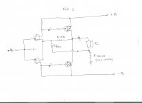
The circuit you show appears to be similar to that in fig. 3 of https://5ad7b68329ae8ddd591c555bf9d.../Loudspeakers_and_negative_impedances-HIk.pdf.
I ran simulations based on that circuit, and found that it would increase damping factor only by floating the power supplies as shown in this schematic. The overall performance based on this circuit looks excellent but it requires one resistor more than the circuit in post #218.
Ihquam
Thanks for very interesting pdf article , I enjoy to read that ,
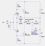
here is another schematic where R-fbs now is not connected to ground line but on `hot` side of R-sense ,
I think now with carefully chosen ratio of values R-vfb , R-fbs and R-sense in relation with some real LS it can be found optimum VFB vs CFB ratio ,
actually I think that most easy way is to change value of R-sense in several steps but only after is established desired hard ratio of R-vfb vs R-fbs , where R-fbs is connected to ground line ,
and only than to try with very different several R-sense values from let`s say 0-ohm ( zero CFB) up to 0,47R ( max CFB ).
Attachments
Last edited:
here is another schematic where R-fbs now is not connected to ground line but on `hot` side of R-sense ,
Maybe, but NP said that only one resistor was added for positive feedback, and this is two.
Banat
In My younger days I built radio receiver circuits featuring a type of positive feedback . They were called regenerative receivers because they sent a controlled amount of the output in phase back to the input such that the signal would be boosted each pass through the circuit.
diyF6 may be game to mine your application via its Jensen transformer.
Ihquam
Thanks for very interesting pdf article , I enjoy to read that ,
here is another schematic where R-fbs now is not connected to ground line but on `hot` side of R-sense ,
I think now with carefully chosen ratio of values R-vfb , R-fbs and R-sense in relation with some real LS it can be found optimum VFB vs CFB ratio ,
actually I think that most easy way is to change value of R-sense in several steps but only after is established desired hard ratio of R-vfb vs R-fbs , where R-fbs is connected to ground line ,
and only than to try with very different several R-sense values from let`s say 0-ohm ( zero CFB) up to 0,47R ( max CFB ).
Yes, that circuit has the desired resistor count and will work if the power supply floats at the top of the Rsense resistor as shown here. I have managed to find resistor values that appear to meet specifications, but a few questions remain:
- Are there noise issues w.r.t. floating power supply
- The -3dB point is very high at around 3MHz.
Attachments
Maybe, but NP said that only one resistor was added for positive feedback, and this is two.
No. If you do not count the 2 resistors at the JFET inputs, there are only 5 resistors, which is the number Nelson got: 4+1.
Maybe, but NP said that only one resistor was added for positive feedback, and this is two.
Well NP is real amp designer I`m just TV mechanicus ( repair man )
") ,
, BTW , just for information each CRT-TV`s vertical deflection amplifiers must have CFB loop to thermally compensate vertical deflection yoke coil , without CFB compensation vertical amplitude ,linearity and many other parameters will be very unstable ,
CFB by audio amps can also compensate thermal compression effect of LS .
Yes, that circuit has the desired resistor count and will work if the power supply floats at the top of the Rsense resistor as shown here. I have managed to find resistor values that appear to meet specifications, but a few questions remain:
- Are there noise issues w.r.t. floating power supply
- The -3dB point is very high at around 3MHz.
I think that R-sense connected in that way altogether with floating PSU introduce CFB to whole amp circuit ,
but I`m wonder why circuit from my post #243 can not work properly ?
- nothing is wrong to have floating PSU
- for -3db point at very high ~3Mhz I have no answer .
Ihquam
Thanks for very interesting pdf article , I enjoy to read that ,
here is another schematic where R-fbs now is not connected to ground line but on `hot` side of R-sense ,
I think now with carefully chosen ratio of values R-vfb , R-fbs and R-sense in relation with some real LS it can be found optimum VFB vs CFB ratio ,
actually I think that most easy way is to change value of R-sense in several steps but only after is established desired hard ratio of R-vfb vs R-fbs , where R-fbs is connected to ground line ,
and only than to try with very different several R-sense values from let`s say 0-ohm ( zero CFB) up to 0,47R ( max CFB ).
Hello banat.
How will you characterize the power output, and the frequency response etc. of your diyF7? Will you drive a loudspeaker in your schematic to xy Watts?
I think that R-sense connected in that way altogether with floating PSU introduce CFB to whole amp circuit ,
but I`m wonder why circuit from my post #243 can not work properly ?
- nothing is wrong to have floating PSU
- for -3db point at very high ~3Mhz I have no answer .
When I simulated your circuit in post #243 the damping factor decreased with increasing feedback thru Rfbs. If you look at the circuit ZM posted in fig. 3 of #236, the transformer secondary connection has the same effect as floating the power supply in my circuit, which inverts the sense of the current thru Rfbs.
Hello banat.
How will you characterize the power output, and the frequency response etc. of your diyF7? Will you drive a loudspeaker in your schematic to xy Watts?
Hello Antoinel
Precise answers I can give you but only after I made and measure real results of my diyF7 amp .
Yes, that circuit has the desired resistor count and will work if the power supply floats at the top of the Rsense resistor as shown here. I have managed to find resistor values that appear to meet specifications, but a few questions remain:
- Are there noise issues w.r.t. floating power supply
- The -3dB point is very high at around 3MHz.
Please see US 4,467,288. This invention is by James Strickland who teaches lowering distortion of an audio power amp [maybe the Trans Nova breed] by using negative and positive feedback.
When I simulated your circuit in post #243 the damping factor decreased with increasing feedback thru Rfbs. If you look at the circuit ZM posted in fig. 3 of #236, the transformer secondary connection has the same effect as floating the power supply in my circuit, which inverts the sense of the current thru Rfbs.
Yes that is the original goal , to lower DF via CFB loop up to `critical DF point` is reached .
Yes that is the original goal , to lower DF via CFB loop up to `critical DF point` is reached .
Yes, that was the goal of that (old) article, but in Nelson's F7 the goal is to increase the damping factor from around 7 to 100, thus requiring a feedback signal of opposite phase.
Yes, that was the goal of that (old) article, but in Nelson's F7 the goal is to increase the damping factor from around 7 to 100, thus requiring a feedback signal of opposite phase.
Well , different people can have very different LS and very different goals
At this point I have to alternalive schematics: posts #218 and #246 which can apparently be made to meet the F7 specifications and have only 4+1 resistors, not counting the 2 JFET input resistors. One requires that both speaker terminals are active, while the other requires that the power supplies float. Pick your poison.
I am still mystified by
I am still mystified by
and the fact that both of my circuits have -3dB points above 2MHz rather than 100kHz of the F7 specs. This suggests to me that Nelson has additional components in the input circuit before the JFET gates that lowpass filter the input to -3dB at 100kHz, define the input impedance, and act gate stoppers. There are obvious ways to do that with 2 resistors and one capacitor. But what is the "clever way"?and found a clever way to further reduce the effect of high frequency DAC noise and environmental RF.
diyF6 may be game to mine your application via its Jensen transformer.
Hello Antoinel
I can see where the Jensen transformer provided isolation could be a benefit. Some of the old circuits referenced here that used bridge connections to combine positive and negative feedback into one signal and tube circuits with output transformers open up lots of possibilities. But none of these are elegant, simple circuits that I believe Papa's F7 is. The transformer might prevent the supplies needing to be floated in some variant designs.
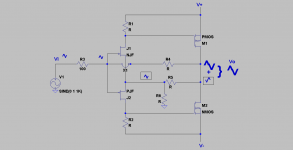
A Concept diyF7
A proposed schematic of a concept diyF7 is attached. It works as follows:
1. Input signal Vi is presented to the joined JFET gates via a 100 Ohm gate stopper resistor.
2. Vi is amplified and appears at the power output node which is in phase with it [i.e.Vi].
3. The first in phase power output signal is returned to the joined JFET gates; which is positive feedback, and further raises the perceived value of the 100 Ohm gate stopper via bootstrap action to a much higher value which is the input impedance of the amp..
4. The first power output signal is next downsized [in rectangle] and then presented to the joined JFET sources which process it as the JFETs operate in common gate configuration.
5. The resultant power output signal [in rectangle] is a consequence of negative feedback, and is out of phase with first output signal due to the amplified Vi
6. The two output signals from the two operating ways of the JFETs, add up to generate a net power output signal [Vo] which is in phase with the input signal Vi.
7 Thus two power output signals were summed; one from a positive and the second from a negative feedback routes.
8. The value of the 3 feedback resistors need to be defined.
9. The amp's voltage gain and its Zi plus other given performance specs can generate simultaneous equations to solve for the value of the 3 resistors.
Best regards
Attachments
- Home
- Amplifiers
- Pass Labs
- First Watt F7 review