Chip,
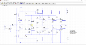
I did a LTSpice simulation of the F4 and have attached the schematic with operating voltages and currents.
First check of the JFETs in place would be to check the voltage drop across the source resistors R3 and R4. Using Ohm's Law:
resistor = 22.1R, current = 5mA, V = 5mA x 22.1R = 111 mV
So measure the voltage drop across R3 and R4.
Remember to include the unit of measure with the numerical value.
The LTSpice schematic also shows voltages at various points that you can use for comparision with your board.
Note that voltages less than 1mV (in the uV, nV, pV range) in the simulation should be considered as zero Volt.
Attachments
Last edited:
Ben,
I was called away but now I'm back on duty.
"First check of the JFETs in place would be to check the voltage drop across the source resistors R3 and R4. Using Ohm's Law:
resistor = 22.1R, current = 5mA, V = 5mA x 22.1R = 111 mV"
When you say across - I have one lead on R3 and the other on R4, with that I get:
R channel: 105.8mV
L Channel 0.0 mV
Does that mean I should pull the Left JFETS and check for signs of life?
Thanks,
Chip
Chip,
Please don't pull any jfets yet.
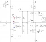
I believe Ben meant that you make two voltage measurement on each channel, one with the probes across R3, and another with the probes across R4. (Please see attached. For R3, put probes at the red circles. For R4, the blue circles).
Doing these 4 measurements (2 per channel) should will give you indications
of the states of the four jfets.
Dennis
Please don't pull any jfets yet.
I believe Ben meant that you make two voltage measurement on each channel, one with the probes across R3, and another with the probes across R4. (Please see attached. For R3, put probes at the red circles. For R4, the blue circles).
Doing these 4 measurements (2 per channel) should will give you indications
of the states of the four jfets.
Dennis
Attachments
Left channel at 0V is not good. It means electrons are not flowing.
But first, across resistor means one meter lead at one end of the resistor and the other meter lead at the other end of the resistor. So please measure across R3 and measure across R4 of the left channel (two separate measurements).
But first, across resistor means one meter lead at one end of the resistor and the other meter lead at the other end of the resistor. So please measure across R3 and measure across R4 of the left channel (two separate measurements).
Ok, here we go:
R3 R4 [all values in mV]
Right 106.8 107.0
Left 0.0 0.0
Left Right
R3 0.0 107.0
R4 0.0 106.8
R3 R4 [all values in mV]
Right 106.8 107.0
Left 0.0 0.0
Left Right
R3 0.0 107.0
R4 0.0 106.8
Last edited:
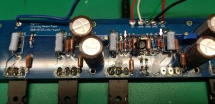
The 0V at the left channel is not good. Just to make sure that the JFETs are getting power to their drain, measure the voltage at R6 relative to ground and at R7 relative to ground. I have marked up your photo with the locations for measuring the voltage. If you get somewhere around 17 to 18V or up to 23V, then there is power to the JFETs and the JFETs are likely not good.
Remove the JFETs and test them. The measured current should be around 10mA or so if they are good.
Remove the JFETs and test them. The measured current should be around 10mA or so if they are good.
Attachments
Last edited:
Ben,
Thanks for this.
I've tried googling, but I still don't understand "relative to ground" so not sure how to place the leads.
Thanks for this.
I've tried googling, but I still don't understand "relative to ground" so not sure how to place the leads.
Ok, but what do I use as ground? I've tried several places, e.g., washers on Mosfets, metal frame, only to get OL on the working right channel.
Thanks,
Thanks,
There are three ground connections points, "GND", on the board between the "In" and "OUT" that you can use.
New readings for R6 & R7 all mV
Left channel 6.6 & 31.4
Right channel 2.6 & 1.02
So it looks like next step is to test the JFETS in left channel.
Thanks
Left channel 6.6 & 31.4
Right channel 2.6 & 1.02
So it looks like next step is to test the JFETS in left channel.
Thanks
Your numbers do not look right.
On your good channel you should get approximately 17V to 18V at R6 relative to ground and at R7 relative to ground. If you measure the other side of the resistor, you should get about 4.5V relative to ground.
On your good channel you should get approximately 17V to 18V at R6 relative to ground and at R7 relative to ground. If you measure the other side of the resistor, you should get about 4.5V relative to ground.
ok, new measurements all V
R6 R7
Left 15.46 -15.32
Right -19.8 20.16
All the values from measuring the other sife of the resistors were around 4.1
So, now on to the Left Jfets?
R6 R7
Left 15.46 -15.32
Right -19.8 20.16
All the values from measuring the other sife of the resistors were around 4.1
So, now on to the Left Jfets?
Last edited:
Something strange is going on.
Your left channel is not working and you did not get any voltage drop across the JFET source resistors R3 and R4. So no electrons were flowing through the JFETs' drain to source, and therefore less electrons were flowing through R5, R22, and P2, and should result in less voltage drop. Therefore I would expect the voltage at R6 and R7 for the left channel to be higher than for the working right channel. But you are reporting the opposite.
Did you get the R6 R7 voltage readings for the channels mixed up?
Or the other possible route for the electrons is from JFET drain to gate and then to ground. You can check for that by measuring the voltage "across" R1. If there is voltage across R1, then that is the case and the JFETs are no good for sure.
The 4.1V on the other side of R6 and R7 indicates that the TL431 bias circuit is working properly, which is good.
Apart from the weird Voltages, the JFETs appear suspect.
New readings for R and R7 [V values] just to make sure I read the correct values by resistor
Left 20.17 and -19.18
Right 15.76 and -15.12
No reading from R1
So on to the Jfets.....
Left 20.17 and -19.18
Right 15.76 and -15.12
No reading from R1
So on to the Jfets.....
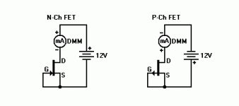
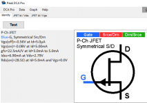
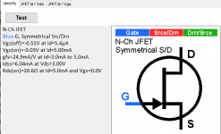
Well, the Jfets are functioning, see attached printouts from my Peak Atlas DCA75 Pro.
I guess I'm stumped. In a previous review I tested all the resistors on the left circuit board and they are correct and functioning. Maybe I should test them again? They all look good.
I guess I'm stumped. In a previous review I tested all the resistors on the left circuit board and they are correct and functioning. Maybe I should test them again? They all look good.
Attachments
Last edited:
Well, the Jfets are functioning, see attached printouts from my Peak Atlas DCA75 Pro.
I guess I'm stumped. In a previous review I tested all the resistors on the left circuit board and they are correct and functioning. Maybe I should test them again? They all look good.
I guess I'm stumped. In a previous review I tested all the resistors on the left circuit board and they are correct and functioning. Maybe I should test them again? They all look good.
Attachments


- Home
- Amplifiers
- Pass Labs
- A guide to building the Pass F4 amplifier