Perhaps you have some bad solder joints. Check the underside of the board for bad solder joints, especially around R3 and R4. It could have been bad solder joint or joints at the JFETs also although it's too late to check that.
It doesn't hurt to reflow the joints in the area.
Since the JFETs test OK, reinstall them, making sure that they are in their correct positions before soldering, and see if it works.
It doesn't hurt to reflow the joints in the area.
Since the JFETs test OK, reinstall them, making sure that they are in their correct positions before soldering, and see if it works.
I understand the frustration. On the positive side you have probably learned a lot. I know I do every time I stumble across issues…
I’ve been thinking you should reflow whatever looks suspicious, like Ben says. But what about your PCB traces? Any sign of lifted or suspicious traces? Any particular joint in the path that you may have unsoldered or resoldered several times?
I wish you good luck! You have stamina, and IME that will get you there in the end.
Cheers,
Andy
Yep. Learning a good deal.
Not complaining, just dogged in pursuit of the truth - where did I muck things up?
Traces look good. I addressed the solder points.
Will put it back together, bias it up and try again.
Thanks for the kind words.
Chip
Not complaining, just dogged in pursuit of the truth - where did I muck things up?
Traces look good. I addressed the solder points.
Will put it back together, bias it up and try again.
Thanks for the kind words.
Chip
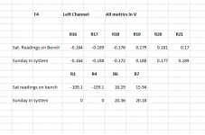
Sunday Update
Yesterday I put everything back together on F4 left channel. New bias.
And took readings on my bench.
Everything looked good.
Today I put the F4 in my system.
Still no sound out of the left channel.
And no readings from R3 & R4
See attached chart.
Not sure next steps.
Yesterday I put everything back together on F4 left channel. New bias.
And took readings on my bench.
Everything looked good.
Today I put the F4 in my system.
Still no sound out of the left channel.
And no readings from R3 & R4
See attached chart.
Not sure next steps.
Attachments
Strange. It tested good yesterday but not good today.
I assume there was nothing connected to the input while on the test bench yesterday.
Was something connected to the input when you took the measurements today?
I assume there was nothing connected to the input while on the test bench yesterday.
Was something connected to the input when you took the measurements today?
Nothing was connected yesterday on the bench.
Today I feed a signal from my preamp, which works fine into my F6.
Puzzled.
Today I feed a signal from my preamp, which works fine into my F6.
Puzzled.
So today's measurements were made with the preamp connected and on?
Try measuring again with nothing connected and see if you can get yesterday's results.
Try measuring again with nothing connected and see if you can get yesterday's results.
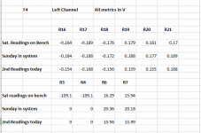
Voltages at R6 and R6 are different in your latest chart so there is a change.
Or are they errors?
Or are they errors?
Unless the new R6 and R7 values are in error, they suggest additional current draw
missing in the "Sunday in system" measurements. I would think the front end is
the natural place where that's coming from that is inconsistent with the reported
R3 and R4 voltages of zero.
missing in the "Sunday in system" measurements. I would think the front end is
the natural place where that's coming from that is inconsistent with the reported
R3 and R4 voltages of zero.
Voltages at R6 and R6 are different in your latest chart so there is a change.
Or are they errors?
You are correct. Those are new readings.
I was more focused on NC in R3 & R4
I have a feeling this is some simple thing I've mucked up....
Not clear - the new numbers are correct? No voltage drop across R3 and R4, 15.94V at R6 and 15.99V at R7 are correct?
Or is it 20.36V at R6 and 20.18V at R7?
Or is it 20.36V at R6 and 20.18V at R7?
R6 = 15.94 R7 = 15.99 were the last readings I took, after I unplugged everything from the F4.
Those voltages are low considering that you measured no voltage drop across R3 and R4. The low voltages at R6 and R7 point to current flowing somewhere, but no voltage across R3 and R4 says that the current is not flowing through the JFETs. So where is it going?
You measured normal voltages when it was on the bench but now the voltages are not good. So something has changed. But before taking it apart again it is time to take a whole bunch of measurements to get a bigger picture.
Please take voltage measurements ACROSS the following:
R1, R3, R4, R5, R6, R7, R8, R9, R22, R24, R25, D3, D4.
Also measure the voltage at R6 and R6 relative to ground again.
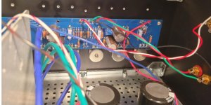
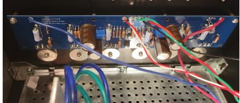
Also some focused and detailed pictures of the board and amplifier please. At least one good picture of the overall layout showing input jack and whole board too.
You measured normal voltages when it was on the bench but now the voltages are not good. So something has changed. But before taking it apart again it is time to take a whole bunch of measurements to get a bigger picture.
Please take voltage measurements ACROSS the following:
R1, R3, R4, R5, R6, R7, R8, R9, R22, R24, R25, D3, D4.
Also measure the voltage at R6 and R6 relative to ground again.
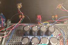
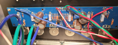
Also some focused and detailed pictures of the board and amplifier please. At least one good picture of the overall layout showing input jack and whole board too.
Ben,
Ok. I will get to work. In the mean time, here are some photos. For some reason I couldn't get them to upload yesterday.
And thanks for the help.
Chip
Ok. I will get to work. In the mean time, here are some photos. For some reason I couldn't get them to upload yesterday.
And thanks for the help.
Chip
Attachments
Those voltages are low considering that you measured no voltage drop across R3 and R4. The low voltages at R6 and R7 point to current flowing somewhere, but no voltage across R3 and R4 says that the current is not flowing through the JFETs. So where is it going?
You measured normal voltages when it was on the bench but now the voltages are not good. So something has changed. But before taking it apart again it is time to take a whole bunch of measurements to get a bigger picture.
Please take voltage measurements ACROSS the following:
R1, R3, R4, R5, R6, R7, R8, R9, R22, R24, R25, D3, D4.
Also measure the voltage at R6 and R6 relative to ground again.
Also some focused and detailed pictures of the board and amplifier please. At least one good picture of the overall layout showing input jack and whole board too.
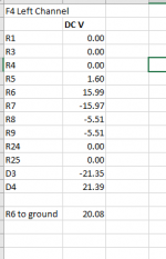
See attached chart for values
Attachments

I haven't read the whole saga, but to me that looks like faulty or reversed jfets. You're not getting any flow through them.
Chip,
Previously when you gave the voltage at R6 and R7, were they relative to Ground as I had asked in post #2707 (A guide to building the Pass F4 amplifier.)?
When I ask for voltage "at" a location, that would be relative to Ground. When I ask for voltage "across" a component, that would be at the component with one probe at each end of the component.
Please measure the voltage at R7 relative to Ground (as shown in post #2707). I had a typo in my previous post and asked for R6 and R6 when I intended R6 and R7.
The voltage drops across R5, R6, and R7 indicate approximately 1.6mA of current in consumed by the front end circuit. That is consistent with the front end current draw with the JFETs not turning on and not working.
Looking at the latest measurements, the voltages across D3 and D4 look low. That voltage should be equal to the power supply voltage. Please measure the V+ and V- voltages relative to Ground, and the voltages at both sides of R1 relative to Ground.
If your power supply voltages measure +/-21.4V, then the voltages across D3 and D4 are equal to the power supply voltages as they should be, and if the voltages at R1 relative to ground is zero, then the voltages to the JFETs are good. The bad is that the JFETs are not turning on even though they are provided with the proper voltages.
The bad news would be that the JFETs don't appear to be working even though you had tested them when they were off the board and that they seemed to be working when you bench tested the channel after reassembly.
So then the possible reason is bad solder joints or bad JFETs.
- Home
- Amplifiers
- Pass Labs
- A guide to building the Pass F4 amplifier