Hi both - & thanks for your helpful & useful feedbacks. I will just ponder what you are saying and get back sometime next week. Wishing you a pleasant weekend ;-)
Cheers,
Jesper
Cheers,
Jesper
I haven't read the datasheet of AD7134 in detail yet. But 1536kps(probably passible) is worth trying because front-end LPF is easy to design even if your target is 20kHz BW or 40kHz. High sampling doesn't always mean wide BW. It has the advantage if DUT has a bit of large HF noise. Some DSM DACs, including mine, sometimes have different SNR between low OSR(x64) and high. If you use high sampling ADC, it's easy to eliminate such RF noise without analog LPF. Four ADCs at 1536kps is interesting.
@xx3stksm: Hi again ... & thanks again for your comments about the AD7134 - which I have been thinking about. And it seems to me that in terms of using it for sound recordings (which would be my purpose) the MCLK of 48 MHz is a "challenge" ...
48 MHz translates to 1496 ksps or divisions of this (e.g. 374 ksps) and, if I calculate this correctly ;-), a 1536 ksps would mean that it should be fed a clock of 49.28 MHz to sample at 1.536 MHz (in line with your thinking I also assume that the less than 3% sampling frequency increase is passable for the AD7134 itself). And it appears that this frequency is not standard - at least from doing a google search and searching Mouser.
I reckon though, that it could be derived from a combination of other frequencies or, if a low phase noise is desired, be custom made (or some other way of doing this) ... ?
Anyway, while thinking about this I also came to think about why it is that you have not yourself designed an ADC that is as you desire it to be? I realize that here I am looking from the outside but having seen what you have accomplished with your DAC, and thinking that you have a very solid practical and theoretical knowledge in these fields - how come that you have not designed e.g. a DS ADC yourself (if I may ask, of course)?
@Tfive: My feeling is that the idea of the AD7134 should simmer for just a while, however, if I end up asking e.g. AD about the file format I'll post a reply here should it be useful. But thanks for checking out the SDP-H1 manual ;-)
Cheers to you both,
Jesper
I have read half of the AD7134 datasheet. There is no continuous-time ADC(both DSM and SAR) for audio purposes as long as I know. AD claims several advantages of continuous-time ADC; high antialias ability, no need for S/H, and easy to drive ADC because of resistive input characteristics. The AD7134 is very interesting, though I don't have enough knowledge about continuous-time ADC.
I haven't fully understood the architecture of the AD7134 yet, but the sampling rate is fixed; 24MHz or 12MHz. You can choose whatever output frequency you want as long as below 1496KHz(sinc3 or sinc6 filter). If you apply 768kHz on the ODR pin, you can have 768ksps because the AD7134 has ASRC, which converts 24MHz into 768kHz. The drawback is the bandwidth. You can't have 384kHz, instead 200kHz(sinc3),140kHz(sinc6). If you use a wideband filter, 160kHz BW is available at 374ksps(max frequency with the wideband filter). The sampling frequency is always 24MHz at max. So, I guess 352.8kHz or 384kHz with the wideband filter is the best solution for the audio purpose.
352.8kHz is no problem. 384kHz is probably possible without hacking. If it doesn't work, 360kHz is a legal way to output 384kHz. The AD7134 can output 360kHz with 155kHz BW, then FPGA upconverts 360kHz to 384kHz( 360*(16/15) ). You have 384kHz sampling with 155kHz BW. 768kHz or 1536kHz is also possible. But they are redundant because BW is 155kHz. That's what I'm now thinking about the AD7134.🙂
@xx3stksm: Hmmm ... looks as if you have already been reading more into the AD7134 datasheet than I have ... And, yes, I think it is interesting.
I am not entirely sure I understand the way the AD7134 converter works but I'll see if I can find the time to read more into the datasheet this upcoming Sunday.
BTW in terms of low distortion ADCs: Did you notice the lower-most right corner figure on p. 6 in LTC2378-20's datasheet? If the reference voltage is set correctly, THD figures down to -132/-133 dBs are possible (and might even be further optimized?). The lowest I have seen for an ADC and had it been more than 20 bits it could have been really interesting ...
Cheers,
Jesper
... I reckon there could be newer sources for this but there was a relatively lengthy section in Richard Schreier's book covering the difference between discrete time & continous time sigma-delta converters. I can't remember exactly where in the book but what I took away from it was that one of the types was less sensitive to jitter/phase noise than the other ...The AD7134 is very interesting, though I don't have enough knowledge about continuous-time ADC.
I am not entirely sure I understand the way the AD7134 converter works but I'll see if I can find the time to read more into the datasheet this upcoming Sunday.
BTW in terms of low distortion ADCs: Did you notice the lower-most right corner figure on p. 6 in LTC2378-20's datasheet? If the reference voltage is set correctly, THD figures down to -132/-133 dBs are possible (and might even be further optimized?). The lowest I have seen for an ADC and had it been more than 20 bits it could have been really interesting ...
Cheers,
Jesper
Oups ... forgot the link to the LTC2378-20's datasheet:
https://www.analog.com/media/en/technical-documentation/data-sheets/237820fb.pdf
Jesper
https://www.analog.com/media/en/technical-documentation/data-sheets/237820fb.pdf
Jesper
Thanks for your interesting feedback. Honestly speaking, I used to be a big fan of SAR ADC rather than DSM one. SAR inherently doesn't have quantization noise increase at HF and was superior to DSM on SNR. My previous ADC was the AD7960(SAR 5MHz sampling). The disadvantage I have experienced with SAR is THD. It doesn't mean SAR is inherently not good at THD. I guess my ADC driver isn't excellent enough to achieve the values on the datasheet. I couldn't get rid of some grass at HF. My DAC also wasn't good enough to complain to them.
The LTC2378-20 has excellent performance. But I have no confidence to have such numbers. My previous one (AD7960) was behind it. My current one(AD7768 DSM) is pretty good. How much performance you can get depends on an ADC driver, including front-end LPF, IMO. The wrong selection often ends up poor THD. It's very tricky to find out the best front-end circuit because the input is usually capacitive load. So, I can't stop trying the AD7134, which has a resistive load. The dependency on the front-end must be less. Furthermore, it is almost aliasing free. Only continuous-time one can have such ability. The attached is the AD7134 THD.
The LTC2378-20 has excellent performance. But I have no confidence to have such numbers. My previous one (AD7960) was behind it. My current one(AD7768 DSM) is pretty good. How much performance you can get depends on an ADC driver, including front-end LPF, IMO. The wrong selection often ends up poor THD. It's very tricky to find out the best front-end circuit because the input is usually capacitive load. So, I can't stop trying the AD7134, which has a resistive load. The dependency on the front-end must be less. Furthermore, it is almost aliasing free. Only continuous-time one can have such ability. The attached is the AD7134 THD.
Attachments

Hi again & thank you also for your feedback ;-) ... It seems though that we have somewhat different experiences wrt. SAR ADCs - so a couple of comments:
Some years ago I (& a couple of very helpful & competent programmers) made an ADC based on the LTC2380-24 as I preferred the 24 bit resolution (for sound recordings). The first version of the ADC had only reasonable distortion values (to my memory ~105 dB 2H at a 12 kHz input) which I was not quite satisfied with although the entire "construction" was placed out in the open (no shielding) and - in hindsight - some of the design specifics were sub-optimal.
So I decided to redo the ADC layout and started out by studying Linear Technology's own suggestion for a layout (eval board). And I noticed that they had somehow encapsulated (sort of a guard-ring) the SPI output pin. Wondering if this could make a difference I tried to implement this approach in this second version and (again to my memory) it now had just about -120 dB 2H distortion at the 12 kHz. My thinking about this is that somehow the noise from the SPI pin disturbs either the input pins or the Vref and thus increases distortion.
I have not had the opportunity to get back to the LTC2380-24 layout but my guess/assumption is that with minor tweaks of the layout (and other parameters) even better performance can be reached. E.g. we were at times sampling at 1.536 MHz and thus were pushing the SPI drive to the maximum (actually a bit higher than the 100 MHz specified), and so there wasn't really any noticeable time lapse between the SPI transmission of the previous data sampled and the new input pin sample.
But I actually used LT's suggested input circuitry (resistor and capacitor decoupling network) and then directly fed my Victor 12 kHz oscillator sine wave into this network (Victor's oscillator is about -133 THD at 12 kHz).
The diyaudio member Frex has also reached very good results with SAR converters:
https://www.diyaudio.com/forums/equ...-source-versatile-analyzer-6.html#post5962088
So I think that at least the LT2380-24 can be made to perform very well (I admittedly do not have experience with the AD7960) ...
Also, in terms of SAR compared with DSM I agree with you on the HF quantization noise advantage of the SAR converters. However, I think they may actually have one (maybe more?) "advantage" and that is that they usually just need a quite low frequency conversion clock meaning that oscillators operating at the optimum frequency for low phase noise can be used (according to the diyaudio member Gerhard this is about 5 MHz). IMHO low phase noise is important in sound recording/playback although I have not yet experienced how low it feasibly may be from a sound quality perspective.
I also think it is interesting and as I mentioned I will see if I can find the time to look deeper into the datasheet on Sunday.
Cheers ;-)
Jesper
The LTC2378-20 has excellent performance. But I have no confidence to have such numbers.
How much performance you can get depends on an ADC driver, including front-end LPF, IMO. The wrong selection often ends up poor THD.
Some years ago I (& a couple of very helpful & competent programmers) made an ADC based on the LTC2380-24 as I preferred the 24 bit resolution (for sound recordings). The first version of the ADC had only reasonable distortion values (to my memory ~105 dB 2H at a 12 kHz input) which I was not quite satisfied with although the entire "construction" was placed out in the open (no shielding) and - in hindsight - some of the design specifics were sub-optimal.
So I decided to redo the ADC layout and started out by studying Linear Technology's own suggestion for a layout (eval board). And I noticed that they had somehow encapsulated (sort of a guard-ring) the SPI output pin. Wondering if this could make a difference I tried to implement this approach in this second version and (again to my memory) it now had just about -120 dB 2H distortion at the 12 kHz. My thinking about this is that somehow the noise from the SPI pin disturbs either the input pins or the Vref and thus increases distortion.
I have not had the opportunity to get back to the LTC2380-24 layout but my guess/assumption is that with minor tweaks of the layout (and other parameters) even better performance can be reached. E.g. we were at times sampling at 1.536 MHz and thus were pushing the SPI drive to the maximum (actually a bit higher than the 100 MHz specified), and so there wasn't really any noticeable time lapse between the SPI transmission of the previous data sampled and the new input pin sample.
But I actually used LT's suggested input circuitry (resistor and capacitor decoupling network) and then directly fed my Victor 12 kHz oscillator sine wave into this network (Victor's oscillator is about -133 THD at 12 kHz).
The diyaudio member Frex has also reached very good results with SAR converters:
https://www.diyaudio.com/forums/equ...-source-versatile-analyzer-6.html#post5962088
So I think that at least the LT2380-24 can be made to perform very well (I admittedly do not have experience with the AD7960) ...
Also, in terms of SAR compared with DSM I agree with you on the HF quantization noise advantage of the SAR converters. However, I think they may actually have one (maybe more?) "advantage" and that is that they usually just need a quite low frequency conversion clock meaning that oscillators operating at the optimum frequency for low phase noise can be used (according to the diyaudio member Gerhard this is about 5 MHz). IMHO low phase noise is important in sound recording/playback although I have not yet experienced how low it feasibly may be from a sound quality perspective.
So, I can't stop trying the AD7134, which has a resistive load. The dependency on the front-end must be less. Furthermore, it is almost aliasing free. Only continuous-time one can have such ability. The attached is the AD7134 THD.
I also think it is interesting and as I mentioned I will see if I can find the time to look deeper into the datasheet on Sunday.
Cheers ;-)
Jesper
I agree with you the LTC2380-24 has excellent performance. I guess the problem with the LTC2380-24 is a bit tricky interface if your target is audio purpose. It doesn't have a standard output like IIS; you need some glue logic. Another inherent nature is the price. It costs about $60. I think it's worth investing in, but if you want more than 120dB SNR, paralleling The LTC2380-24 isn't an optimum solution. The LTC2380-24 and recent DSM ADC(AD7768 or AD7134) have almost the same SNR(115dB at 20kHz BW). It's easy to parallel DSM ADC because they are intended to do so. The most inexpensive one is the AD7768($45 with 8 ADCs). IMO, If your target is high SNR with less than 192ksps, DSM is better. If more than 192ksps is mandatory, SAR is better.
@xx3stksm: Thanks again for your comments above.
I had the opportunity to read into the AD7134 datasheet yesterday and I still find it interesting, however, from a sound recording point of view I think it may have some "challenges".
The main one is the ODR (output data rate) functionality which is indeed very flexible but for audio sampling data rates depends on a PLL which - as I have read about it - is pretty hard to design so that it has low phase noise at close-in frequencies (which, as I understand it, is quite key in relation to obtaining very good perceived sound quality).
The second is the INL values which - if I read this correctly - are about three times higher than the similar values for the LTC2380-24. I am not sure if this may in practice correlate with specific sound quality observations but I would imagine that it could affect "non-linear" low-level noise/distortion.
On the other hand I do follow your thoughts - and the AD7134 datasheet's comments - about the simplified input circuitry which would really be a gift ... I have performed measurements on the LTC2380-24's input and IMO/IME it is noisy and depends on appropriate filtering.
Yet, besides the inter-channel timing differences, there are also the potential differences in EMI radiation (crosstalk etc.) in the different channels which makes me slightly "careful" with parallelling channels for audio purposes. I reckon it can be different for measurements, though.
Regarding either of the ADC's price level I do consider it important, however, I have also been thinking that when it comes to the actual recording of e.g. orchestras I have often been a bit sad that so many musicians spend most of their lives practicing and rehearsing this beautiful music just to have it recorded (often) suboptimally. With this in mind I decided that the price of the ADC (unless it was prohibitively expensive) should not be the deciding factor - more so how it would likely perform from a music & sound quality point of view. But, again, I realize that from a measurement point of view things may be different ....
So with our exchange here in the last posts in mind I reckon it is time to just ponder your inputs and the datasheets' information ... and then I also think that it would indeed be great if Analog would consider designing a continuous-time DS ADC which were especially optimized for audio. Like 1536 kHz sampling and divisions of this frequency without a PLL ....
Cheers & thanks again for giving your feedbacks on this 😉
Jesper
I had the opportunity to read into the AD7134 datasheet yesterday and I still find it interesting, however, from a sound recording point of view I think it may have some "challenges".
The main one is the ODR (output data rate) functionality which is indeed very flexible but for audio sampling data rates depends on a PLL which - as I have read about it - is pretty hard to design so that it has low phase noise at close-in frequencies (which, as I understand it, is quite key in relation to obtaining very good perceived sound quality).
The second is the INL values which - if I read this correctly - are about three times higher than the similar values for the LTC2380-24. I am not sure if this may in practice correlate with specific sound quality observations but I would imagine that it could affect "non-linear" low-level noise/distortion.
On the other hand I do follow your thoughts - and the AD7134 datasheet's comments - about the simplified input circuitry which would really be a gift ... I have performed measurements on the LTC2380-24's input and IMO/IME it is noisy and depends on appropriate filtering.
Hmmm... Again from a sound recording perspective: I notice in the AD7134 datasheet that the phase matching between channels is of a magnitude of a couple of nanoseconds. And between ICs just about 10 ns. Just thinking here that normally in audio one is trying to achieve picosecond or femtosecond timings ... (please note that I do not yet have any opinion about the feasibility of this as I have not practical experience with the sound-wise implications of such very low timing (in)differences).It's easy to parallel DSM ADC because they are intended to do so.
Yet, besides the inter-channel timing differences, there are also the potential differences in EMI radiation (crosstalk etc.) in the different channels which makes me slightly "careful" with parallelling channels for audio purposes. I reckon it can be different for measurements, though.
It costs about $60.
Regarding either of the ADC's price level I do consider it important, however, I have also been thinking that when it comes to the actual recording of e.g. orchestras I have often been a bit sad that so many musicians spend most of their lives practicing and rehearsing this beautiful music just to have it recorded (often) suboptimally. With this in mind I decided that the price of the ADC (unless it was prohibitively expensive) should not be the deciding factor - more so how it would likely perform from a music & sound quality point of view. But, again, I realize that from a measurement point of view things may be different ....
So with our exchange here in the last posts in mind I reckon it is time to just ponder your inputs and the datasheets' information ... and then I also think that it would indeed be great if Analog would consider designing a continuous-time DS ADC which were especially optimized for audio. Like 1536 kHz sampling and divisions of this frequency without a PLL ....
Cheers & thanks again for giving your feedbacks on this 😉
Jesper
Last edited:
Regarding the timing differences: These are static I would assume and hence would average out when summing the different ADC signals digitally. This is not to be confused with "jitter" which means non-stationary, random timing errors that will affect the sampling "point in time" and produce non-deterministic errors. In one sentence, I would not worry about them at all. After all 10ns equals a distance of 0.00034 mm of distance at the speed of sound in air. Practically pointless to worry about.
@gentlevoice: Thank you for the comment on the AD7134. Interestingly, you have an entirely different viewpoint from mine.🙂 I'm now designing my AD7768 board for renewal. An ADC driver is the essential circuit to achieve high performance because almost every ADC includes S/H for discrete sampling. S/H is a kind of a trap. The best way to be safe is to eliminate it. So, the AD7134, which doesn't have S/H, is the best for me. The top priority is S/H free.
The second is aliasing. It's not easy to design an antialiasing filter with a high noise rejection and small footprint. I usually use 24.576MHz crystal to be able to synchronous sampling. But many DACs have a relatively large noise spectrum around frequencies divided by N(12.288MHz, 6.144MHz), which ends up aliasing noise. The AD7134, which has high antialias rejection, is a rescue boat again. That's why the AD7134 is my highly recommended chip now. Some disadvantages are the drawback to fix the most critical one. My consideration is based on measurement purposes. If your application is a music recording, I'm sure another selection is better because paralleling ADCs doesn't make sense.
As to PLL, one solution is to use a 45.1584MHz(44.1kHzx1024) crystal, which can drive the AD7134 and divide by N counter is the souse for ODR(no PLL exists). You can easily convert the 44.1kHz family to the 48kHz family in the digital domain(no artifact). The second choice is 48MHz crystal for the AD7134 and 24.576MHz crystal for ODR. Two crystals rarely cause a problem. But I'm sure a four-layer PCB will fix the trouble. I would practically use a 24.576MHz crystal for ODR and 46.8114MHz(24.576x(40/21)) for the AD7134; one crystal. I haven't experienced the PLL jitter problem as long as PLL is appropriately designed. PLLs inside FPGA are high quality because the PLL jitter is probably smaller than the logic gate one: the total is almost 10ps, the physical limit.
@Tfive: I agree with you. Phase skew between ADCs is static. I don't think it pollutes signal quality. IMO, the 1st factor to dominate ADC performance is an ADC driver because most of the time I waste in debugging is front-end circuit. The 2nd is antialiasing, the 3rd is the reference voltage, and the 4th is clock jitter. I'm sure jitter is less critical than many people think if your target is the audio band.
@Tfive: Thanks for your feedback ... I also agree if the channel skew can be considered static or at least quite stable over a relatively long period (like many seconds), e.g. mainly influenced by temperature variations.
@xx3stksm: Hmmmm, yes, it would seem that we have somewhat different priorities in ADC design, although from reading your last posts I reckon that in practice the main difference is the likely effect of jitter (but as I mentioned I have not yet had the chance to make conclusive observations about this).
Will just ponder the rest of your reply & the AD7134.
Cheers & thanks,
Jesper
Last edited:
hi xx3stksm,
I went thru your interesting project rapidly.
I didn't find peculiar stuff to take care about the PS (power supply) of the FPGA.
You use linear regs ? one in front of each Vin of the FPGA ?
At the back of the PCB, I see some caps. Did you use high capacity X-type MLCC ? like 100µF or 220µF in 1210 form factor... based on photo I think not.
As PS of FPGA is critical (next to FPGA Vins, not miles away), high capacitance MLCC X-type is a no-alternative to the curent transcient response linked to FPGA activity.
Thanks for feedback.
Rgds
Hi xx3
Can I ask what is You opinion on sound (and other) when acomplish switching with Transistor stages. And when "switch" with logic complementary mosfet gates (in digital ICs)
IF You have some experiance I would be aperaciate to hear please...Because You are using dikrate BJT stages at the output of Your device.
I am asking because i somehow not satisfied with driving R2R nets direct from digital IC gates...
And probably I wiould like to try something like this:
Attachments

Last edited:
hi xx3stksm,
I went thru your interesting project rapidly.
I didn't find peculiar stuff to take care about the PS (power supply) of the FPGA.
You use linear regs ? one in front of each Vin of the FPGA ?
At the back of the PCB, I see some caps. Did you use high capacity X-type MLCC ? like 100µF or 220µF in 1210 form factor... based on photo I think not.
As PS of FPGA is critical (next to FPGA Vins, not miles away), high capacitance MLCC X-type is a no-alternative to the curent transcient response linked to FPGA activity.
Thanks for feedback.
Rgds
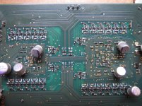
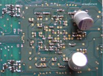
I guess the photo you saw was not my DAC but my ADC. The attached pics are the bottom side of my 1bit DSM DAC. As you said, bypassing the FPGA power supply is essential. I usually assign bypass caps(0.1uF,0402) on the bottom side to be as close to power pins as possible(GND is a solid inner plane). Track length of power is almost 1mm. Only the bottom side can achieve such an ideal condition. Without bypass caps, you can find some degradation on SNR. The drawback is too many vias. They are an obstacle to route inner BGA pads. That's the reason I can't use less than 0.8mm BGA.
Attachments
Hi xx3
Can I ask what is You opinion on sound (and other) when acomplish switching with Transistor stages. And when "switch" with logic complementary mosfet gates (in digital ICs)
IF You have some experiance I would be aperaciate to hear please...Because You are using dikrate BJT stages at the output of Your device.
I am asking because i somehow not satisfied with driving R2R nets direct from digital IC gates...
And probably I wiould like to try something like this:
Your attached pic is probably R2R(PCM) ladder DAC architecture. It's possible to drive R2R both with a discrete logic(HC590) and with a differential amplifier(your pic). But 1bitDSM with a differential amplifier is a bit different from the R2R ladder. One tap of 1bitDSM is independent of others: one is already complete DAC. Paralleling taps means averaging to achieve better performance. A discrete device(HC590) is also configured as 1bitDSM. All the more reason to avoid a discrete one for me is noise performance. You can't get rid of noise from the power rail because no PSRR exists as long as you use discrete logic. If you use a differential amplifier instead of discrete logic, you have some PSRR because it acts as a current switch. I don't know why some 1bitDSM can have excellent SNR despite discrete logic. I guess it's their secret.
As to the sound quality, I haven't finished soldering eight DACs which is necessary for my system. What I can say is if you are a classical music listener, poor SNR is fatal. That's the reason why I design 1bitDSM with a differential amp. I have some experience with poor SNR 1bitDSM. It's terribly bad for music with pianissimo.🙁
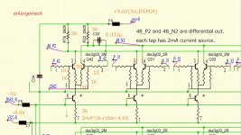
Could you elaborate a bit more on the pecl output stage of yours, maybe show a little more of the schematic. What I'd be interested to learn is (references are to the schematic of the original post on page one):
- what's the bias signal for? do have transistors have to be matched closely when fed from a shared bias signal?
- are r2/r3 half the value of r5/r6 to avoid imbalances in the loading of the output currents?
- what are the voltage values on vcc-8 and vcc_cl?
- what are r1/r4 for? do they provide a basic current path and you shunt away parts of it with the transistors?
maybe you could enlighten us all. What I find very interesting is that this scheme seems to avoid most of the fluctuations of the current draw on the reference voltage line as it's basically always the same except during the switching transistions. I'd image that relaxes the requirements for the analog voltage supply quite a bit compared to multibit output stages like the ess chips have for example (with zero psrr and current draw following the modulator/audio signal).
Last edited:
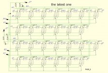
The latest analog section(pic.1 and pic.2) is slightly different from post #1. No specific bias is required because FPGA I/O swings from zero to 1.3V. I have measured several hundred transistors' Vbe and found no significant difference; no need to select. Beta is ignorable if Vbe is the same in a differential stage by a transistor.
The converted signal across R78 and R22 has only a simple op-amp buffer; no op-amp differential stage now. If you use a discrete device(HC590) instead of transistors, it's very tricky to have excellent SNR. I tried it several times but failed and gave up such architecture. Replacing HC590 with transistors also failed. Many trials and errors couldn't bring me a successful result: the zero PSRR trap.🙁 That's the reason I have reached transistor-based differential amp.
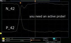
P_42 and N_42 are differential pairs driven by FPGA I/O. Three transistors differential amp is non-saturation switching architecture, where no current fluctuation exists except transition time: the shorter transition, the better. FPGA I/O has many options, slew rate, drive power, and swing voltage. Pic.3 is probably the best scenario. Less than one nano sec transition time with slight ringing is very challenging. I'm sure only FPGA I/O can complete the job because it has enough VCC and GND pads to output a stable pulse.
Furthermore, an internal PLL can adjust the skew between positive and negative output by 0.1 nano sec. Such preciseness implies better jitter performance; probably 30 pico at max. The skew is entirely a critical factor to have perfect conversion. Fast and ringing less switching with fine adjustment is the point to have excellent performance.
The converted signal across R78 and R22 has only a simple op-amp buffer; no op-amp differential stage now. If you use a discrete device(HC590) instead of transistors, it's very tricky to have excellent SNR. I tried it several times but failed and gave up such architecture. Replacing HC590 with transistors also failed. Many trials and errors couldn't bring me a successful result: the zero PSRR trap.🙁 That's the reason I have reached transistor-based differential amp.
P_42 and N_42 are differential pairs driven by FPGA I/O. Three transistors differential amp is non-saturation switching architecture, where no current fluctuation exists except transition time: the shorter transition, the better. FPGA I/O has many options, slew rate, drive power, and swing voltage. Pic.3 is probably the best scenario. Less than one nano sec transition time with slight ringing is very challenging. I'm sure only FPGA I/O can complete the job because it has enough VCC and GND pads to output a stable pulse.
Furthermore, an internal PLL can adjust the skew between positive and negative output by 0.1 nano sec. Such preciseness implies better jitter performance; probably 30 pico at max. The skew is entirely a critical factor to have perfect conversion. Fast and ringing less switching with fine adjustment is the point to have excellent performance.
Attachments
- Home
- Source & Line
- Digital Line Level
- My no DAC project, FPGA and transistors