Hi Ian, maybe this question has been answered already, but nevertheless....
1. Is the FIFO relying on word clock = 64x bit clock, i.e. 32bit for each channel? Or does it clock out WS the same as is clocked in, independently of length of the word clock (i.e. from 16 to 32 bits).
Please note, I'm not talking about how many bits the data word has....
2. If, for example, I'd like to stop the bit clock after 20 bits of data until the next WS transition, would, at the exit of the FIFO, the bit clock stop too?
Thank you for your support!
Tino
Hi Ian, maybe this question has been answered already, but nevertheless....
1. Is the FIFO relying on word clock = 64x bit clock, i.e. 32bit for each channel? Or does it clock out WS the same as is clocked in, independently of length of the word clock (i.e. from 16 to 32 bits).
Please note, I'm not talking about how many bits the data word has....
2. If, for example, I'd like to stop the bit clock after 20 bits of data until the next WS transition, would, at the exit of the FIFO, the bit clock stop too?
Thank you for your support!
Tino
1. The FIFO output sck will be 64Fs with each channel 32bit no matter how many bits you input for right and left. For example, you can input I2S signal with 16 sck for each channel, but output will still be 32bit 64Fs with the rest LSBs fill in zero.
2. For the FIFO input I2S, you can stop bit clock after 20, the output will play continuoully without any problem. It's FIFO 🙂, the output clock has no business with input clock.
It's the nature of I2S protocol. That's why 16bit I2S signal can be played at 24 bit DAC. Please refer to I2S standard which was linked in the end of user's guide, maybe it's more clear than what I said. 🙂
Good luck with the KIT
You Delta Sigma DAC guys are spoiled 😉
As always, i should have explained why i was asking a question.
OK, that answers almost both questions...the output is not just an exact (and "realigned" in time domain) copy of the three input lines, but stuffed with additional bits on the data line (albeit zeros) and corresponding bit clock, up to 32 bits per channel.
I have to stop the clock, because the DAC i plan to use accepts right justified data, and it is a 20 bit dac. If i do not stop the clock after the first 20 bits, it will clock in another 12. In case of 16 bit audio, i'll get only silence without stopping the clock.
And i thought to stop the clock before the FIFO, avoiding additional logic after it.
AD R2R DAC's (eg AD1862) do not follow the I2S protocol, unfortunately.
Look here for a journey into the good old days: http://www.analog.com/static/imported-files/application_notes/383160163AN207.pdf
With the fifo, I'll delay the word clock 1 BCK before FIFO to align MSB with the word clock, and stop the clock and split left and right data after the FIFO.
As the AD1862 (or AD1865, PCM63 for instance) will trigger conversion based on word clock going negative, word clock jitter performance is to watch for.
But as the needed logic on the word clock line between FIFO and DAC's are only two XOR gates for phase splitting, i think i'll be ok.
Maybe I'll open a separate thread for this.
Thank you anyway
As always, i should have explained why i was asking a question.
1. The FIFO output sck will be 64Fs with each channel 32bit no matter how many bits you input for right and left. For example, you can input I2S signal with 16 sck for each channel, but output will still be 32bit 64Fs with the rest LSBs fill in zero.
OK, that answers almost both questions...the output is not just an exact (and "realigned" in time domain) copy of the three input lines, but stuffed with additional bits on the data line (albeit zeros) and corresponding bit clock, up to 32 bits per channel.
Well, in some cases it's good this way, in some others not...For the FIFO input I2S, you can stop bit clock after 20, the output will play continuoully without any problem. It's FIFO 🙂, the output clock has no business with input clock.
I have to stop the clock, because the DAC i plan to use accepts right justified data, and it is a 20 bit dac. If i do not stop the clock after the first 20 bits, it will clock in another 12. In case of 16 bit audio, i'll get only silence without stopping the clock.
And i thought to stop the clock before the FIFO, avoiding additional logic after it.
I know the I2S protocol....but as i said, you guys with D/S DAC are spoiled.It's the nature of I2S protocol. That's why 16bit I2S signal can be played at 24 bit DAC. Please refer to I2S standard which was linked in the end of user's guide, maybe it's more clear than what I said.
AD R2R DAC's (eg AD1862) do not follow the I2S protocol, unfortunately.
Look here for a journey into the good old days: http://www.analog.com/static/imported-files/application_notes/383160163AN207.pdf
With the fifo, I'll delay the word clock 1 BCK before FIFO to align MSB with the word clock, and stop the clock and split left and right data after the FIFO.
As the AD1862 (or AD1865, PCM63 for instance) will trigger conversion based on word clock going negative, word clock jitter performance is to watch for.
But as the needed logic on the word clock line between FIFO and DAC's are only two XOR gates for phase splitting, i think i'll be ok.
Maybe I'll open a separate thread for this.
Thank you anyway
You Delta Sigma DAC guys are spoiled 😉
As always, i should have explained why i was asking a question.
OK, that answers almost both questions...the output is not just an exact (and "realigned" in time domain) copy of the three input lines, but stuffed with additional bits on the data line (albeit zeros) and corresponding bit clock, up to 32 bits per channel.
Well, in some cases it's good this way, in some others not...
I have to stop the clock, because the DAC i plan to use accepts right justified data, and it is a 20 bit dac. If i do not stop the clock after the first 20 bits, it will clock in another 12. In case of 16 bit audio, i'll get only silence without stopping the clock.
And i thought to stop the clock before the FIFO, avoiding additional logic after it.
I know the I2S protocol....but as i said, you guys with D/S DAC are spoiled.
AD R2R DAC's (eg AD1862) do not follow the I2S protocol, unfortunately.
Look here for a journey into the good old days: http://www.analog.com/static/imported-files/application_notes/383160163AN207.pdf
With the fifo, I'll delay the word clock 1 BCK before FIFO to align MSB with the word clock, and stop the clock and split left and right data after the FIFO.
As the AD1862 (or AD1865, PCM63 for instance) will trigger conversion based on word clock going negative, word clock jitter performance is to watch for.
But as the needed logic on the word clock line between FIFO and DAC's are only two XOR gates for phase splitting, i think i'll be ok.
Maybe I'll open a separate thread for this.
Thank you anyway
Hi Man,
I suspected your are using AD1865, and now I got the confirm!
Actually, I like the sound of AD1865. I'm listening to it everyday from my PCM-7040 DAT (I connect a S/PDIF FIFO to it 🙂 ). So,you see, I'm still not 100% be spoiled 😛.
For it doesn't support I2S format, to interface AD18xx DAC with my FIFO, there are two solutions:
1. Design an interface board converting the I2S stream into AD18xx format.
2. Integrating that interface into the FPGA/CPLD on the FIFO board.
I'm looking forward to your new thread to see what kind of help I can provide,
Best regards,
Being in the AD1865 interface boat I found interesting the proposal of integrating the AD18xx interface into the FPGA but unfortunately it doesn't seems feasible for me. At least one inverter is still needed to differentiate between L/R word selects and the 11.34us delay of the right channel is still there (with 44.1KHz format)For it doesn't support I2S format, to interface AD18xx DAC with my FIFO, there are two solutions:
1. Design an interface board converting the I2S stream into AD18xx format.
2. Integrating that interface into the FPGA/CPLD on the FIFO board.
or do you know how to get a "true" AD18xx format out of the FIFO board: 1 frame select, 2 data lines with data aligned as 18bit LSBJ and 1 clock ? I would be interested 😉
Well that is not really something i care much about. Corresponds to about 4mm sound travel, and is constant over full bandwith.[...]and the 11.34us delay of the right channel is still there (with 44.1KHz format)[...]
As the AD1862 (and 1865, or BB PCM63) do convert the data based on word clock (or Latch Enable LE), it is important to have low jitter on these lines.
Stopping BCK does indeed also help to allow conversion without any other line "polluting" the DAC internals and ground.
I believe, the PMD100 digital filter did something along these lines too.
BCK would be important for PCM1702/1704, as they start conversion 2 or 4 bit clocks after LE going down.
Well that is not really something i care much about. Corresponds to about 4mm sound travel, and is constant over full bandwith.
As the AD1862 (and 1865, or BB PCM63) do convert the data based on word clock (or Latch Enable LE), it is important to have low jitter on these lines.
Stopping BCK does indeed also help to allow conversion without any other line "polluting" the DAC internals and ground.
I believe, the PMD100 digital filter did something along these lines too.
BCK would be important for PCM1702/1704, as they start conversion 2 or 4 bit clocks after LE going down.
Being in the AD1865 interface boat I found interesting the proposal of integrating the AD18xx interface into the FPGA but unfortunately it doesn't seems feasible for me. At least one inverter is still needed to differentiate between L/R word selects and the 11.34us delay of the right channel is still there (with 44.1KHz format)
or do you know how to get a "true" AD18xx format out of the FIFO board: 1 frame select, 2 data lines with data aligned as 18bit LSBJ and 1 clock ? I would be interested 😉
Hi zinsula, Hi vzs,
Both of you made very good point.
1. Stopping the clock after latching 18/20bit data is a very smart idea. It make sense to reduce the noise floor.
2. Latching left and right data at same LE falling edge is another good idea. At least, it could eliminate the 11.34us phase difference between the two channels.
3. Instead of using mclk, AD1865/2,PCM63 use LE launching the conversion, so, it would be better to re-clock those signals with a hi-speed low jitter flip-flop by a good master clock to maximize the performance.
4. Because of the signals feed to those DACs are totally different from I2S, so the converter board should be stand along from the FIFO board which is following the I2S standard.
That would be an attractive project for FPGA/CPLD based design.
Last edited:
Hi Ian,
Finally I integrated the FIFO into my NOS DAC system and did a quick listening session.
With the generic clock, default clock module and simple 74HCxx based circuitry in the AD1865 converter it's already better then before, but I'm too biased now 🙂 I have to listen to it more relaxed for a couple of days to have a better impression. I have in plans to change the clocks and build Demian's regulator for them.
Do you recommend connecting a better regulator to the whole clock module or just to the clocks separately? - as you did while testing with the batteries.
If feeding the whole clock module from a reg like Demain's or Salas' will the on-board ADP151 regulators degrade/increase this ultra-low noise floor?
I would be happy to buy such a pre-programmed IC or even a whole kit project. Do you have in plans to start such a converter project or should I better invest in a bunch shift-registers 🙂 ?
Finally I integrated the FIFO into my NOS DAC system and did a quick listening session.
With the generic clock, default clock module and simple 74HCxx based circuitry in the AD1865 converter it's already better then before, but I'm too biased now 🙂 I have to listen to it more relaxed for a couple of days to have a better impression. I have in plans to change the clocks and build Demian's regulator for them.
Do you recommend connecting a better regulator to the whole clock module or just to the clocks separately? - as you did while testing with the batteries.
If feeding the whole clock module from a reg like Demain's or Salas' will the on-board ADP151 regulators degrade/increase this ultra-low noise floor?
It would be really nice to swap eight ICs with one CPLD/FPGA - four reclocking flip-flops would be needed anyway.4. Because of the signals feed to those DACs are totally different from I2S, so the converter board should be stand along from the FIFO board which is following the I2S standard.
That would be an attractive project for FPGA/CPLD based design.
I would be happy to buy such a pre-programmed IC or even a whole kit project. Do you have in plans to start such a converter project or should I better invest in a bunch shift-registers 🙂 ?
Last edited:
Hi Ian,
Finally I integrated the FIFO into my NOS DAC system and did a quick listening session.
With the generic clock, default clock module and simple 74HCxx based circuitry in the AD1865 converter it's already better then before, but I'm too biased now 🙂 I have to listen to it more relaxed for a couple of days to have a better impression. I have in plans to change the clocks and build Demian's regulator for them.
Do you recommend connecting a better regulator to the whole clock module or just to the clocks separately? - as you did while testing with the batteries.
If feeding the whole clock module from a reg like Demain's or Salas' will the on-board ADP151 regulators degrade/increase this ultra-low noise floor?
It would be really nice to swap eight ICs with one CPLD/FPGA - four reclocking flip-flops would be needed anyway.
I would be happy to buy such a pre-programmed IC or even a whole kit project. Do you have in plans to start such a converter project or should I better invest in a bunch shift-registers 🙂 ?
Can you share your schematic? I can't decide where to use my fifo eith with a pair of AD1862's or a TDA1541. For the AD1862 I was going to send the fifo i2s to a PMD100 and forget NOS due to the complexity of format conversion. A CPLD that did the conversion and L/R split would be ideal for the NOS crowd we have been left out in the cold with asynch usb and basically any means to have a master clock at the DAC short of as you say 8+ IC's which tends to make one question if we gain much by forgoing the oversampling filter. A CPLD/FPGA for NOS'ers would be a godsend.
I think I'll open a thread, as I have some ideas, but with "traditional" logic.
It would convert from I2S with 32bit frames as this FIFO spits out, to the right justified data the AD1862 and ..65 needs.
AD1862 being different to AD1865 in that it accepts 20bit depth.
Bit lenght could be even switched i think.
The solution i have in my head would not "interrupt" the Word Clock line with logic, nor it would be necessery to reclock it, so to maintain the essential jitter performance as good as it comes out from FIFO.
However, we would need to tap WCK as it serves as a Flag for BCK stopping and directing into the correct channel (L/R).
So we can "oversample" via software, save the Files as eg. 192/20 (or whatever the DAC chip can accept), and play it via USB or S/PDIF. The FIFO will reduce the jitter as good as it gets, AND spit out a single format without having to take into account bit depth or whatever.
TDA1541A would not need any modification of this FIFO output, as it accepts I2S.
This is the I2S to LSBJ converter I'm using: linkCan you share your schematic?
Note to the schematics: the MCK divide by 2 is not needed, you can simply reclock with MCK so only 5 ICs are needed. The data lines for L and R are shared and the word latches are distinct. The actual pcb schematics I used is here: link . I removed the MCK divider from it and added a U-FL connector for the MCK. You could either do this on breadboard or I could send you the gerbers.
As you see I wasn't aware to use high frequency flip-flops for reclocking nor to comply with LVTTL systems. You should use 74HCT ICs, I used 74HC so I had to lower the supply voltage to 4V to have VIH low enough. If you need more info about this schematics/build let's move to the thread where I posted it.
I took the main idea from Eric Juaneda's decoder: link and slightly modified it.I think I'll open a thread, as I have some ideas, but with "traditional" logic.
It would convert from I2S with 32bit frames as this FIFO spits out, to the right justified data the AD1862 and ..65 needs.
AD1862 being different to AD1865 in that it accepts 20bit depth.
Bit lenght could be even switched i think.
The solution i have in my head would not "interrupt" the Word Clock line with logic, nor it would be necessery to reclock it, so to maintain the essential jitter performance as good as it comes out from FIFO.
This can convert a 64bit I2S stereo sample into the preferred bit depth LSBJ format. The reclocking of Word Clock is mandatory to have everything in sync but will not degrade at all because it is done with the MCK from FIFO (as on FIFO's clock module).
I have to listen to it more relaxed for a couple of days to have a better impression.
My suggestion for a listening test using the FIFO, whether you are 100% isolated from the (jittery) source or not:
a) use original CD an music with many room information (Jazz, Blues etc)
b) rip the a) CD and burn them on a (carbon) CD-R using 1:1 speed or even using master mode speed (old Yamaha F1 do this) or paint the CD-R edges green with a permanent marker.
if you identify any differences then ooooh.... dear.... it will not be your last tweak O😉
Cheers
Hp
(carbon) CD-Rs are my favorite, they sound almost like vinyl without the harsh digital sound of el-cheapo bulk CDs. I already tried different colors for carbon CD-R edges but for me orange is the non-plus-ultra. It gives a warm, tubey sound, without being harsh, also spacial information is so good that I can not only hear Norah Jones in front of me but I can fuzzily see her. 😱My suggestion for a listening test using the FIFO, whether you are 100% isolated from the (jittery) source or not:
a) use original CD an music with many room information (Jazz, Blues etc)
b) rip the a) CD and burn them on a (carbon) CD-R using 1:1 speed or even using master mode speed (old Yamaha F1 do this) or paint the CD-R edges green with a permanent marker.
if you identify any differences then ooooh.... dear.... it will not be your last tweak O😉
Cheers
Hp
CREEK CD50 MK2 CD PLAYER
Fifo buffer was used in the Cane Creek CD50 MK2 with great results.
https://docs.google.com/viewer?url=http%3A%2F%2Fwww.elusivedisc.com%2Fcreekcd50review.pdf
Fifo buffer was used in the Cane Creek CD50 MK2 with great results.
https://docs.google.com/viewer?url=http%3A%2F%2Fwww.elusivedisc.com%2Fcreekcd50review.pdf
Hi Ian,
Finally I integrated the FIFO into my NOS DAC system and did a quick listening session.
With the generic clock, default clock module and simple 74HCxx based circuitry in the AD1865 converter it's already better then before, but I'm too biased now 🙂 I have to listen to it more relaxed for a couple of days to have a better impression. I have in plans to change the clocks and build Demian's regulator for them.
Do you recommend connecting a better regulator to the whole clock module or just to the clocks separately? - as you did while testing with the batteries.
If feeding the whole clock module from a reg like Demain's or Salas' will the on-board ADP151 regulators degrade/increase this ultra-low noise floor?
It would be really nice to swap eight ICs with one CPLD/FPGA - four reclocking flip-flops would be needed anyway.
I would be happy to buy such a pre-programmed IC or even a whole kit project. Do you have in plans to start such a converter project or should I better invest in a bunch shift-registers 🙂 ?
Very good progress. What I'm suggesting is:
1. Get a really nice lock first, it will make you distinguishing the good power supply.
2. Based on my own experience, feeding batteries into the reg and feeding them directly into the oscillator (without reg) dosen't make much difference. However, feeding a ac based regulated dc supply into the reg was making big difference. You already know what I mean 🙂.
The most significant problem is, the rectifiers are actually working at switching mode. Your could even receiving that rectifying noise from a short wave radio! Fast recovery diodes are better, but still can't eliminate those rectifying noise 100%. That noise comes with very high bandwidth extending to couple of GHz, no regulator could supress them very well. Multi-order CLC filters are working, but you have to design them with carefull to catch up with batteries.
Having more fun with your project
Regard
I think I'll open a thread, as I have some ideas, but with "traditional" logic.
It would convert from I2S with 32bit frames as this FIFO spits out, to the right justified data the AD1862 and ..65 needs.
AD1862 being different to AD1865 in that it accepts 20bit depth.
Bit lenght could be even switched i think.
The solution i have in my head would not "interrupt" the Word Clock line with logic, nor it would be necessery to reclock it, so to maintain the essential jitter performance as good as it comes out from FIFO.
However, we would need to tap WCK as it serves as a Flag for BCK stopping and directing into the correct channel (L/R).
So we can "oversample" via software, save the Files as eg. 192/20 (or whatever the DAC chip can accept), and play it via USB or S/PDIF. The FIFO will reduce the jitter as good as it gets, AND spit out a single format without having to take into account bit depth or whatever.
TDA1541A would not need any modification of this FIFO output, as it accepts I2S.
This is the I2S to LSBJ converter I'm using: link
Note to the schematics: the MCK divide by 2 is not needed, you can simply reclock with MCK so only 5 ICs are needed. The data lines for L and R are shared and the word latches are distinct. The actual pcb schematics I used is here: link . I removed the MCK divider from it and added a U-FL connector for the MCK. You could either do this on breadboard or I could send you the gerbers.
As you see I wasn't aware to use high frequency flip-flops for reclocking nor to comply with LVTTL systems. You should use 74HCT ICs, I used 74HC so I had to lower the supply voltage to 4V to have VIH low enough. If you need more info about this schematics/build let's move to the thread where I posted it.
Thank you so much for sharing your ideas. You make things getting more and more interesting. If I did this projcet, I'd like to use a CPLD.
1. It will cover both AD1865(18bit) and AD1862(20bit), as well as PCM63(20bit).
2. Accept I2S signals with sck from 48Fs to 64Fs. left and right justified, maybe.
3. Shifting left and right data into registers at same time and stop clk after doing that to reduce noise further more.
4. Launching left and right channel conversion at same moment to eliminate the phase difference.
5. All signals will be re-clocked by a high-speed low jitter flip-flop with the FIFO master clock before feeding into DAC.
6. Support DAC working at both stereo and mone mode.
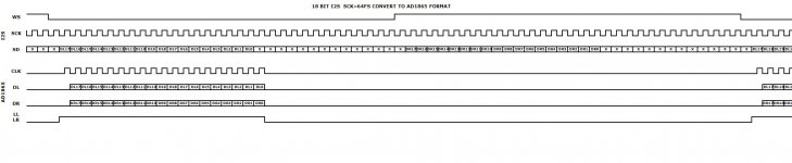
I attched the possible timing waveform (take AD1865 for example). Please let me know if there is any problem.
Cheers,
Ian
Attachments
Last edited:
Well,
as mentioned in #333. Listening tests with different jittery CD/CD-R's you will get the trough! While Marl Levinson used this technique years ago and they did not prove using the mentioned bench test.
While I did also more then 15 years ago a PIC controlled crystal DACVCO (almost a free running) and had finally the same issue and then my project went ^^^....
Currently I deal with my setup Wadia 851 CD with Glas Link, modified Wadia 27 DAC, modified Cary SL-100 monoblocks & Magnepan 3.6 and have the big differences (some more some less) between those CD/CD-R's and even playing the same wave file trough a RME Babyface & optical link. As soon times comes trough I would like to measure (using D-Jitter signals or else...) and see what happens... that's why I build my measurement SW 😀
Hp
Fifo buffer was used in the Cane Creek CD50 MK2 with great results.
https://docs.google.com/viewer?url=http%3A%2F%2Fwww.elusivedisc.com%2Fcreekcd50review.pdf
as mentioned in #333. Listening tests with different jittery CD/CD-R's you will get the trough! While Marl Levinson used this technique years ago and they did not prove using the mentioned bench test.
While I did also more then 15 years ago a PIC controlled crystal DACVCO (almost a free running) and had finally the same issue and then my project went ^^^....
Currently I deal with my setup Wadia 851 CD with Glas Link, modified Wadia 27 DAC, modified Cary SL-100 monoblocks & Magnepan 3.6 and have the big differences (some more some less) between those CD/CD-R's and even playing the same wave file trough a RME Babyface & optical link. As soon times comes trough I would like to measure (using D-Jitter signals or else...) and see what happens... that's why I build my measurement SW 😀
Hp
[...]
I attched the possible timing waveform (take AD1865 for example). Please let me know if there is any problem.[...]
Sounds good Ian!
One suggestion: Please delay LL and LR (Latch Enable) going down one or more clocks after loading the data and stopping clock. So everything is quiet when the Chip does the conversion.
The other thing being, you cannot use this scheme with PCM1702/1704, as they need the Bit Clock running constantly. They do the conversion 2 or four bits after LE going down.
Not a problem for those using the AD or PCM63 converters, this is just to point that out.
- Home
- Source & Line
- Digital Line Level
- Asynchronous I2S FIFO project, an ultimate weapon to fight the jitter