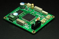
People keep talking too much about jitter issues, but did less to make some kind of improvement. I decided trying to do something real – a working asynchronous I2S FIFO.
Before I go any further, I need to make something clear in advance:
1. FIFO is widely believed as one of the final methods to deal with jitter problems. But the asynchronous FIFO itself is just a technology which could provide a logic function to isolate the two clock domain. That means, for an I2S stream, digital audio data could pass through without any modification but the input clock was blocked and replaced with the new one. The new clock is totally independent from the old one except they should have the similar frequency. The FIFO logic itself does not influence the sound quality;
2. What really makes it sound better (or even worse) is the low jitter secondary clock. For example, if we have a new clock after the FIFO which comes with one digit ps jitter(RMS), we should get much better sound quality than before (the jitter level of the master clock from DIR chip usually around 50ps(RMS) level above corner frequency). So, we should pay more attention on the secondary clock and related interface. Everything connected to secondary clock has to be very carefully to deal with; otherwise new additive jitter will be introduced;
3. The size of the FIFO memory should big enough to meet overflow or empty time caused by the worst case of i2s input clock, but still has to be carefully selected to get the balance between the delay time caused by the working depth(usually half full) of the FIFO;
4. FIFO with low jitter secondary clock could only reduce the play back jitter for an audio DAC, but has nothing to do with the sampling jitter. I don’t have any idea if a CD was reordered with poor clock of the ADC.
The main logic functions could be achieved by a FPGA/CPLD chip together with a megabit SRAM. But the clock section has to use specialized clock/timing circuit, because the jitter performance of the output of FPGA/CPLD are far from what we want.
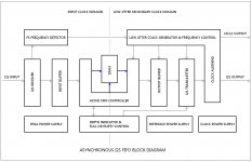
Below is the possible block diagram of this I2S FIFO project:
https://github.com/iancanada/DocumentDownload
https://twitter.com/iancanadaTT
FifoPi Q7 Jan.12,2023 update https://github.com/iancanada/DocumentDownload/blob/master/FifoPi/FifoPiQ7/FifoPiQ7Manual.pdf
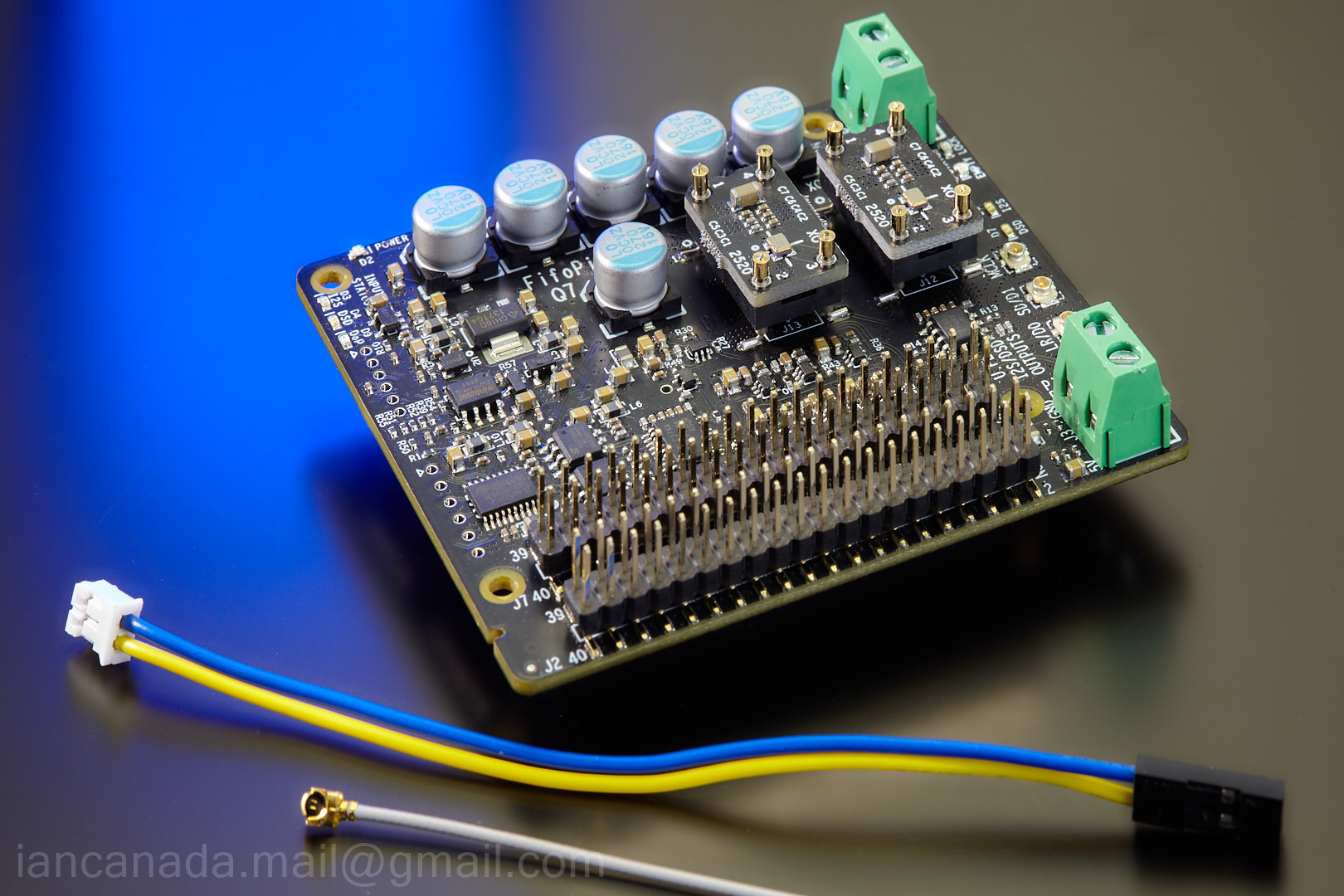 FifoPiQ7_0 by Ian, on Flickr
Before I go any further, I need to make something clear in advance:
1. FIFO is widely believed as one of the final methods to deal with jitter problems. But the asynchronous FIFO itself is just a technology which could provide a logic function to isolate the two clock domain. That means, for an I2S stream, digital audio data could pass through without any modification but the input clock was blocked and replaced with the new one. The new clock is totally independent from the old one except they should have the similar frequency. The FIFO logic itself does not influence the sound quality;
2. What really makes it sound better (or even worse) is the low jitter secondary clock. For example, if we have a new clock after the FIFO which comes with one digit ps jitter(RMS), we should get much better sound quality than before (the jitter level of the master clock from DIR chip usually around 50ps(RMS) level above corner frequency). So, we should pay more attention on the secondary clock and related interface. Everything connected to secondary clock has to be very carefully to deal with; otherwise new additive jitter will be introduced;
3. The size of the FIFO memory should big enough to meet overflow or empty time caused by the worst case of i2s input clock, but still has to be carefully selected to get the balance between the delay time caused by the working depth(usually half full) of the FIFO;
4. FIFO with low jitter secondary clock could only reduce the play back jitter for an audio DAC, but has nothing to do with the sampling jitter. I don’t have any idea if a CD was reordered with poor clock of the ADC.
The main logic functions could be achieved by a FPGA/CPLD chip together with a megabit SRAM. But the clock section has to use specialized clock/timing circuit, because the jitter performance of the output of FPGA/CPLD are far from what we want.
Below is the possible block diagram of this I2S FIFO project:
https://github.com/iancanada/DocumentDownload
https://twitter.com/iancanadaTT
FifoPi Q7 Jan.12,2023 update https://github.com/iancanada/DocumentDownload/blob/master/FifoPi/FifoPiQ7/FifoPiQ7Manual.pdf
 FifoPiQ7_0 by Ian, on Flickr
Attachments
Last edited:
Hello!
When I was reading this I was really excited, that is exactly what I am "waiting for". Unfortunately I am far too bad, far too green to contribute anything, I wish I could. I really hope your FIFO project is making progress, really looking foward to following this thread, all the best!
When I was reading this I was really excited, that is exactly what I am "waiting for". Unfortunately I am far too bad, far too green to contribute anything, I wish I could. I really hope your FIFO project is making progress, really looking foward to following this thread, all the best!
Hi florianderton, thank you for your reply.
Me too. I'v been waiting for this kind of toy for many years. That is why finially decided to make it by myself. Using the I2S FIFO, you could upgrade your DAC, your CD player, Sound card and everything related the I2S or SPDIF stream with the better external clock, and you don't have to put up with the DIR recover clock any more. Hopefully I could bring you some good news step by step. I'd be happy to share the DIY experience with you guys. Welcome feedbacks. Ian
Me too. I'v been waiting for this kind of toy for many years. That is why finially decided to make it by myself. Using the I2S FIFO, you could upgrade your DAC, your CD player, Sound card and everything related the I2S or SPDIF stream with the better external clock, and you don't have to put up with the DIR recover clock any more. Hopefully I could bring you some good news step by step. I'd be happy to share the DIY experience with you guys. Welcome feedbacks. Ian
Sorry for the late update. I’d like this I2S FIFO has the following features:
1. The FIFO section
.Memory size: 4MB;
.FIFO half-full delay time: 0.743 seconds (for 44.1 KHz Fs);
.Half-full over flow time: 1486 seconds (at 44.1KHz input I2S stream with 500ppm frequency tolerance);
.Smart depth control strategy is integrated.
2. The I2S input section
.3.3V LVTTL logic input level with 5V TTL tolerance;
.Support 44.1KHz, 48KHz,88.2KHz, 96KHz,176.4KHz,192KHz Fs;
.Accept 16bit, 24bit, 32bit definition.
3. The I2S output section
.3.3V LVTTL logic output level with 5V TTL tolerance;
.Support 44.1KHz, 48KHz,88.2KHz, 96KHz,176.4KHz,192KHz Fs;
.keep output definition as same as the input stream;
.Master clock frequency: 128*Fs, 256*Fs (default) or 512*Fs.
4. The low jitter clock generator section
.Clock section is a standalone daughter board with the rubber ring hook up;
.Master clock will output via coax cable and separated from I2S connector;
.Clock board is upgradeable and could be easily replaced with the different type of clock/timing solutions to experience the different taste;
.Multi-frequency clock board support Fs automatically switching function;
.Might comes with I2S re-clock function;
.Might support external clock only mode with clock board free;
.Different type of clock board may develop and available for different applications or different users.
5. Extension
.Could interface with the DIR/DIT board to become a SPDIF FIFO;
.LVDS/ECL I2S output support is under consideration.
6. Power supply
.6V/500mA DC input power supply. Could also be easily powered by a standard 6V rechargeable battery for the better performance;
.On board CLC filter;
.Independent ultralow noise, high PSRR LDOs equipped for each sections of the circuit.
Still something might be missing?…..I guess J
This project is not that much complicated, but still a lot of jobs and a lot of details. Some of them are done and some are still undergoing.
The Verilog HDL coding seems a bit boring, but it’s very fundamental to the project. Modules by module, state by state, signal by signal, have to go through everything one by one. CPLD/FPGA design going across two clock domains has to be tested with careful. Both functional and timing simulation is very important to make sure design target is achieved before running the real hardware.
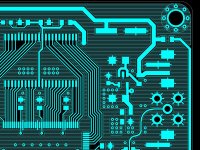
PCB layout is my favorite job. Not only because it makes you feel like very close to the actual board, but also it’s a kind of artwork.
I just got the prototype PCBs last weekend and I’m busy assembling them right now. I’m pretty sure I could show something on the next post.
Attachments
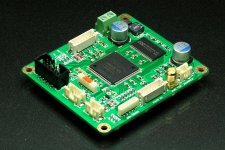
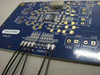
I just finish assembling the I2S FIFO board. A lot of SMT components. By using some little tools, it’s still OK for hand assembling, not that much difficult. So, finally I could show you some pictures of the board. This board has an I2S input, an I2S output and a clock input port. It could be driven by an external master clock or working together with a standalone clock board. This is a brand new clock and has no any business with input I2S signals. I’m gonna test it the next step. Just cross your finger.
Attachments
Last edited:
Very nice job and you have made progress very fast.
Is this your core job/business or is it only hobby?
Does this project have any commercial sight?
Is this your core job/business or is it only hobby?
Does this project have any commercial sight?
Thanks Egberttheone. I'm a R&D engineer. My job focuses on medical electronics. But I’m an audiophile also. In the past couple decades of years, I did quite a few audio projects, include tube/solid amplifiers, CD transports, antique/full range speakers, DACs, PC HIFI and something else. Now, what I’m interested in the most is the digital audio. I always believe we should get the better sound if we could do something perfect. Talking about commercial operating, I don’t have much idea right now. It quite depends. It depends on what the performance it could achieve and what kind of application it can do. The most important thing is how many people need it. So I think at current stage, I have to focus on the project and try to get more improvement. Have a nice weekend. Ian.
Hi Ian, very interesting indeed!! nice job on the pcb, what size micro coax are you using? ufl or wfl connectors? i ask, because all i2s inputs on my gear is using wfl
never mind, i just spotted the connector on the board, not the 6ghz micro coax smd type i was thinking you might use
Hi Qusp. Thank you for interesting. I figured out what you were talking about. That's very good point. It should be like this: Digi-Key - J983CT-ND (Manufacturer - 128-0711-201) I may try it later on.never mind, i just spotted the connector on the board, not the 6ghz micro coax smd type i was thinking you might use
what I'm useing right now for the mclk on the I2S FIFO board is the SMA RF connector. Ian
Thanks Irakli, I will. Have a nice weekend. IanVery nice job indeed! I wish you published more details.
Thank you so much Woodturner-fran. I'm busy testing the boards. I'll update it as soon as possible. Regards, IanBest of luck with the project - I'm subscribing to this thread!
wow! Ian that is really impressiv how fast this is all going on! I am so surprised and happy about that!) All the best, really excited! Best regards, Florian
Hi Qusp. Thank you for interesting. I figured out what you were talking about. That's very good point. It should be like this: Digi-Key - J983CT-ND (Manufacturer - 128-0711-201) I may try it later on.
what I'm useing right now for the mclk on the I2S FIFO board is the SMA RF connector. Ian
Hey Ian, yeah sorry i should have linked it and i forgot the dot in w.fl, its that type, but the one i'm using is a touch more upmarket, its made by hirose and comes available with double shielded mini coax cables, it looks to be the same, or at least similar connection standard as the one you linked, but its a bit pricier and does seem, or at least looks higher quality. its also described as ultra low coax smd, so perhaps its lower profile.
they really are excellent and handy little connectors, i have also used them just recently for sense/feedback connections for low noise regulators to power my portable dac.
see them on my ackodac AKD12P below, makes for really neat compact connections. they were just hooked up randomly for this pic a while ago now before i stuffed the boards
Attachments
Last edited:
Functional test
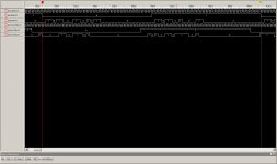
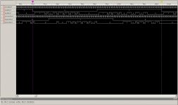
Functional test was done. Everything seems OK, so far so good. The actual timing is almost as same as the simulation result I did a month ago. Some bugs in the Verilog source code have been fixed. Little bit modification on PCB will be shown at the next version. Here are some details.
1. I2S Timing test
44.1Khz 16bit: PASS
48Khz 16bit: PASS
88.2Khz 24bit: PASS
96Khz 24bit: PASS
192Khz 24bit: PASS
2. Bit perfect test
2^32 times 32bit data comparison, no error found
3. I2S FIFO delay test
0.89s for 44.1K I2S stream between input and output with FIFO depth around half full (could you put up with it?)
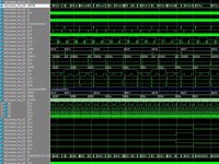
The attached pictures are the testing result from a logic analyzer. Just for reference. It shows very clear that the input sck and ws has nothing to do with the output sck and ws on timing.
The next step gonna be the playing test.
Attachments
Last edited:
looks good, though that delay, if needed any time you switched tracks in an album is a bit annoying, though i guess unavoidable?
I2S FIFO delay test 0.89s for 44.1K I2S stream between input and output with FIFO depth around half full (could you put up with it?)
Actually yes. But why not more memory to increase the 1486 seconds?
Think anyone can live with more delay.
And with highres material, i guess the 1486 seconds is a lot less...
Do you detect "silences" between songs and allow the fifo to go to half full again (remove/add some silence)?
But indeed interesting. Seems easier than trying to build an extra pll 😀
- Home
- Source & Line
- Digital Line Level
- Asynchronous I2S FIFO project, an ultimate weapon to fight the jitter
