Lutkeveld: the onboard stam32F030 does not have a SAI.
However, I currently listens to music through a Nucleo F7 board that implements:
- asynch USB,
- DSP filtering,
- output 4 channels on SAI (Spdif mode)
This feeds 2x Fx-audio D802 amplifiers.
But it is not my intention to put a Stm32F4 or Stm32F7 uC on this design.
Thanks about the explanations for the registers sizing.
JMF
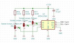
About the schematics for the Eeprom, the draft is as below.
As several boards can be daisy chained on the I2C, I propose to provide all the flexibility for Eeprom addresses via solder jumpers
As space starts to be scarce, I wonder if:
- R45, R46 are needed, or if I could have only one R45 to potentially connect A0, A1 and A2 to +3.3V ?
- Do I really need the 3 way solder jumpers to connect either to +3.3V or GND; or the internal pull down is sufficient (datasheet allows for floating pins (read as 0), but advices to have connections) ?
JMF
Attachments
About the schematics for the Eeprom, the draft is as below.
As several boards can be daisy chained on the I2C, I propose to provide all the flexibility for Eeprom addresses via solder jumpers
As space starts to be scarce, I wonder if:
- R45, R46 are needed, or if I could have only one R45 to potentially connect A0, A1 and A2 to +3.3V ?
- Do I really need the 3 way solder jumpers to connect either to +3.3V or GND; or the internal pull down is sufficient (datasheet allows for floating pins (read as 0), but advices to have connections) ?
JMF
You don't need those resistor, you can connect directly to VDD or GND, but you have to take care of the pull up resistors in parallel on SDA and SCL line when adding slave boards.
You don't need those resistor, you can connect directly to VDD or GND, but you have to take care of the pull up resistors in parallel on SDA and SCL line when adding slave boards.
Thanks AIM65 for the reply.
I will be happy to suppress the pull-up resistors. However the datasheet https://datasheet.lcsc.com/szlcsc/Microchip-Tech-AT24C256C-SSHL-T_C6482.pdf
states:
Device Addresses (A2, A1, A0): The A2, A1, and A0 pins are device address inputs that are hard wired (directly to GND or to VCC) for compatibility with other Atmel AT24C devices. When the pins are hard wired, as many as eight 256K devices may be addressed on a single bus system. (Device addressing is discussed in detail in Section 7. “Device Addressing” on page 9). A device is selected when a corresponding hardware and software match is true. If these pins are left floating, the A2, A1, and A0 pins will be internally pulled down to GND. However, due to capacitive coupling that may appear during customer applications, Atmel recommends always connecting the address pins to a known state. When using a pull-up resistor, Atmel recommends using 10k or less.
So ambiguous about "Directly connected" and "When using a pull-up resistor, Atmel recommends using 10k or less"
Do you confirm I can suppress ?
About paralleling the pull-up resistors on I2C lines when having several boards in serie, any advice ? Currently they are 10kR. Intention would be to have the possibility to daisy chain un to 4 boards (let's say 4 ways stereo speaker) => Any advice on this ?
Last, about the supervisor function, I thought that TI engineers knew what they were doing. The circuit is intended to monitor +12V and VDD with one single analog input that should stay below 3.3V. I tried to understand how R40, C54, C55, R41 and R42 work together but did not succeed. Help welcomed.
Best regards,
JM
Hello JM,
I usually follow manufacturer recommendations and I haven’t seen such recommendation by other suppliers of 24C256: ST or OnSemi. But this is not big stake.
You’ll have 4 I2C pullup in parallel, a quick check should be made, there’re many app notes available on Internet in order to compute min and max pullup values according to number of devices, speed, capacitive load, etc…
For the PSU monitor, no doubt they knows what they do ! , question was to understand what they intend to measure with such a circuit. Now, I believe their solution allows to monitor the value of +12 rail and only the major negative variations of VDD rail such as a VDD drop. About their circuit, I’ve no idea why they have 3 caps in // (1u + 100n + 100n) and not a single one. Resistor value are certainly calculated for +12 and +36V and also for the threshold value of the TPS3802, they should be revised for other value than 36V. It'll be interesting to run an LTSPice analysis to confirm waveform and values in case of VDD drop. It'll give you a idea of what Uc software should do in order to manage reset. If I find some time...
Chris
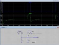
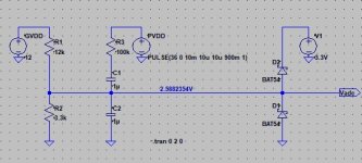
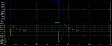
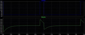
PSU monitor sim
The first sim with LTspice shows that current resistor set the operating point much too high (3.4V), any drop and return on PVDD will destroy the Uc (signal goes up to 4.2V). As proposed this should be clamped to 3.3 and GND with Schottkys. The TPS3802 is certainly protected, not the STM32
Having a single 1u cap rather than 3 for 1.2u and changing one resistor will set the operating point to 2.5V.
I ran sim for two different PVDD drop : first one from 36V to 20V during 100ms the second other from 36V to 0 during 800 msec.
If you set your software threshold to 2.2V you’ll catch them both, even in repetitive condition.And 2.2V threshold is also reached when GVDD (the +12V) reach 8.9V.
This setup should be ok, and it is not linked to PVDD value, only on the variation of PVDD.
Pic from left to right : current values, target value circuit, 100ms drop, 800ms drop
Attachments
So I have updated the schematics and the PCB for the voltage monitoring part according to AIM65 proposal.
Is it OK to use SS15 Shottky diodes (SMA - https://datasheet.lcsc.com/szlcsc/1903051003_MDD-Jiangsu-Yutai-Elec-SS14_C2480.pdf) instead of the suggested ones, except for the size ? It is the "smaller" JLCPCB basic part for Schottky diode.
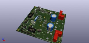
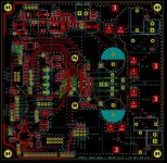
Attached the latest schematics and some pictures.
JMF
Is it OK to use SS15 Shottky diodes (SMA - https://datasheet.lcsc.com/szlcsc/1903051003_MDD-Jiangsu-Yutai-Elec-SS14_C2480.pdf) instead of the suggested ones, except for the size ? It is the "smaller" JLCPCB basic part for Schottky diode.
Attached the latest schematics and some pictures.
JMF
Attachments
Last edited:
Note that I intend to use Unisonic Tech LM2940G-12V-AA3-R (https://datasheet.lcsc.com/szlcsc/Unisonic-Tech-LM2940G-12V-AA3-R_C127023.pdf) instead of TI LM2940.
I could also use AMS1117-3.3 (https://datasheet.lcsc.com/szlcsc/1811201117_Advanced-Monolithic-Systems-AMS-AMS1117-3-3_C6186.pdf) instead of TI TLV1117-33IDCYR
I could also use AMS1117-3.3 (https://datasheet.lcsc.com/szlcsc/1811201117_Advanced-Monolithic-Systems-AMS-AMS1117-3-3_C6186.pdf) instead of TI TLV1117-33IDCYR
Hi
Shottkys are choosed for their lower forward voltage. At JLCPB you have BAS40-04 which is a dual one. SS15 are power devices. If dual ones are not available as basic device, we can order then solder them apart.
LM2940, from UTC, yes, same for AMS117, those chips are everywhere! check 1117 pinout I had bad experience as a replacement of LM1117.
If I may, it’ll nice to have a serial connector (Tx,Rx and GND) connected to Uc, this will allow to use cheap usb2serial adapter and eventually be able to use Lutkeveld host software…
Chris
Have added the BAS40-04 in place of the 2 power Schottky diodes.
Replaced the TLV1117-33IDCYR by the AMS1117-3.3 (same pinout)
I also fitted a small 1mm pitch pin header for a serial link:
1- USART1_RX
2- USART2_TX
3-GND
Maybe not perfect, but here if someone needs serial connectivity.
This Stm32F0 packs packs nice features in 0.8€, and the fact to be able to configure the functions on different pins helps implementation.
JMF
Hello,
To finalize the board, I had a second thought to try to replace for main connectors the pin headers(Dupont) by JST XH connectors. Those have a 2.5mm pitch, similar to 2.54 mm pinheader but not exactly the same. It seems OK for few pins, but to make problems starting from some number.
However, it looks like the most common hobbyist connector, possible to crimp easily, found at good prices.
Feedback appreciated:
- wether it is a good or bad idea to try to replace main connectors from pin headers (Dupont) to JST-XH ?
- for up to how many pins it is still compatible with 2.54 pin headers pattern ?
JMF
Last edited:
Decision to stay in Dupont connectors. This is the easier to find, male / female, all sizes.
Last, which "clearance" needed for the "post assembly" soldering of the TAS3251. My intention is drag soldering with a C2 soldering tip. There are two capacitors that are 2mm away from the center of the TAS3251 footprint pads. This may not be sufficient. I see three options:
- move the Capacitors a bit further (3mm) ?
- not populate those 2 caps, solder the TAS3251, then solder the caps,
- use another technique for the "post soldering" of the TAS3251.
Any advice ?
JMF
So, one move forward. I have ordered 10 boards to JLCPCB. Let's now wait for news.
I made some free space about key connectors to allow people to chose their preferred ones. The remaining components to populate are as expected. The board has the 24C246, the stm32F0, LM5010, LM2940, AMS1117-3.3, all top side 0805 and 0603 minus one, most SMT alu caps minus one.
If everything goes as expected for the taxes, the price will arrive at 15€ per board + shipping booked now (before tested and demonstrated as working).
Interested persons were (please confirm or decline):
- 1xDoctormord,
- 2xAIM65
- 2xXRK91
- 2xCapt Grogg
- 3 JMF
Go 🙂
JMF
Last edited:
Update:
- 2xAIM65 (Confirmed)
- 1xDoctormord,
- 2xXRK91
- 2xCapt Grogg
- 3 JMF
- Waiting list:
2x KaffiMann
1x Onefabis (MP on the 23/01/2020)
- 2xAIM65 (Confirmed)
- 1xDoctormord,
- 2xXRK91
- 2xCapt Grogg
- 3 JMF
- Waiting list:
2x KaffiMann
1x Onefabis (MP on the 23/01/2020)
So, the board appears "under production" on JLCPCB website. I ordered from Aliexpress some Dupont connectors, terminal blocks.
For board connectors, they are all 0.1 pitch. For my prototype, I will go for basic male pin headers. I bought a pack of female Dupont connectors of the different formats for the cables. Will work except that this don't provide keys to control orientation... For soùme of them there is enough room to use Molex_KK-254_AE-6410 which are 0.1 pitch.
I also has a look at the remaining components. The ones that seems available only in one location is the heatsink (ATS-TI1OP-519-C1-R3 Advanced Thermal Solutions Inc. | Fans, Thermal Management | DigiKey)
I had in mind that that specific model was needed because of the "shoulder" on the bottom, to clear from components on the side. However, it seems thad the bigger SMD caps are 1.6mm high, and the TAS3251 chip seems 2.3 mm over the PCB. So maybe a more basic heatsink could do the job.
Do any of you have experience with heatsinks for those chips and the best way to proceed? If the "shoulder is needed or not (I saw fome picture of "reworked" heatsink on Doctormord website) ?
Best regards,
JMF
Seems that I have not chosen the best time to send my order to JLCPCB. The boards are "In Production". But not much progress on the website about the assembly sequence.
Wait and see...
So I started to have a look at the software part, and started installing CubeMX IDE + connecting a stm32 blue pill board.
JMF
Wait and see...
So I started to have a look at the software part, and started installing CubeMX IDE + connecting a stm32 blue pill board.
JMF
Last edited:
Seems that I have not chosen the best time to send my order to JLCPCB.
Chinese New Year
- Home
- Amplifiers
- Class D
- [design log] Neat 2x170W I2S in, I2C controlled, integrated DSP amp (TAS3251)